Supercharge Your Innovation With Domain-Expert AI Agents!

Bit line control circuit for semiconductor memory device

a control circuit and memory device technology, applied in the field of semiconductor memory devices, can solve the problems of difficult to amplify a large amount of cell data, and achieve the effect of preventing the voltage level of a vcore terminal from rapidly increasing

Active Publication Date: 2007-03-29
SK HYNIX INC
View PDF7 Cites 4 Cited by
  • Summary
  • Abstract
  • Description
  • Claims
  • Application Information

AI Technical Summary

Benefits of technology

[0006] It is, therefore, an object of the present invention to provide a semiconductor memory device for preventing a voltage level of a VCORE terminal from rapidly increasing when a bit line sense amplifier operates an overdriving operation in an environment of a relatively high external voltage.

Problems solved by technology

However, it is difficult to amplify a large amount of cell data for a short time by using the core voltage (VCORE) in the low voltage environment.

Method used


Image

  • Bit line control circuit for semiconductor memory device
  • Bit line control circuit for semiconductor memory device
  • Bit line control circuit for semiconductor memory device

Examples


first embodiment

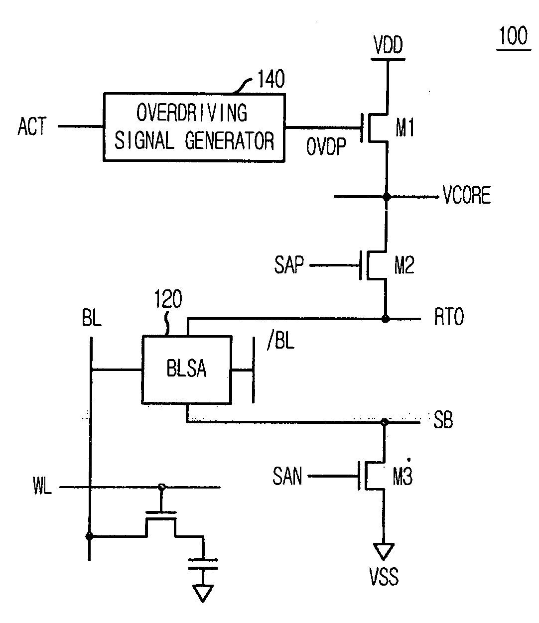
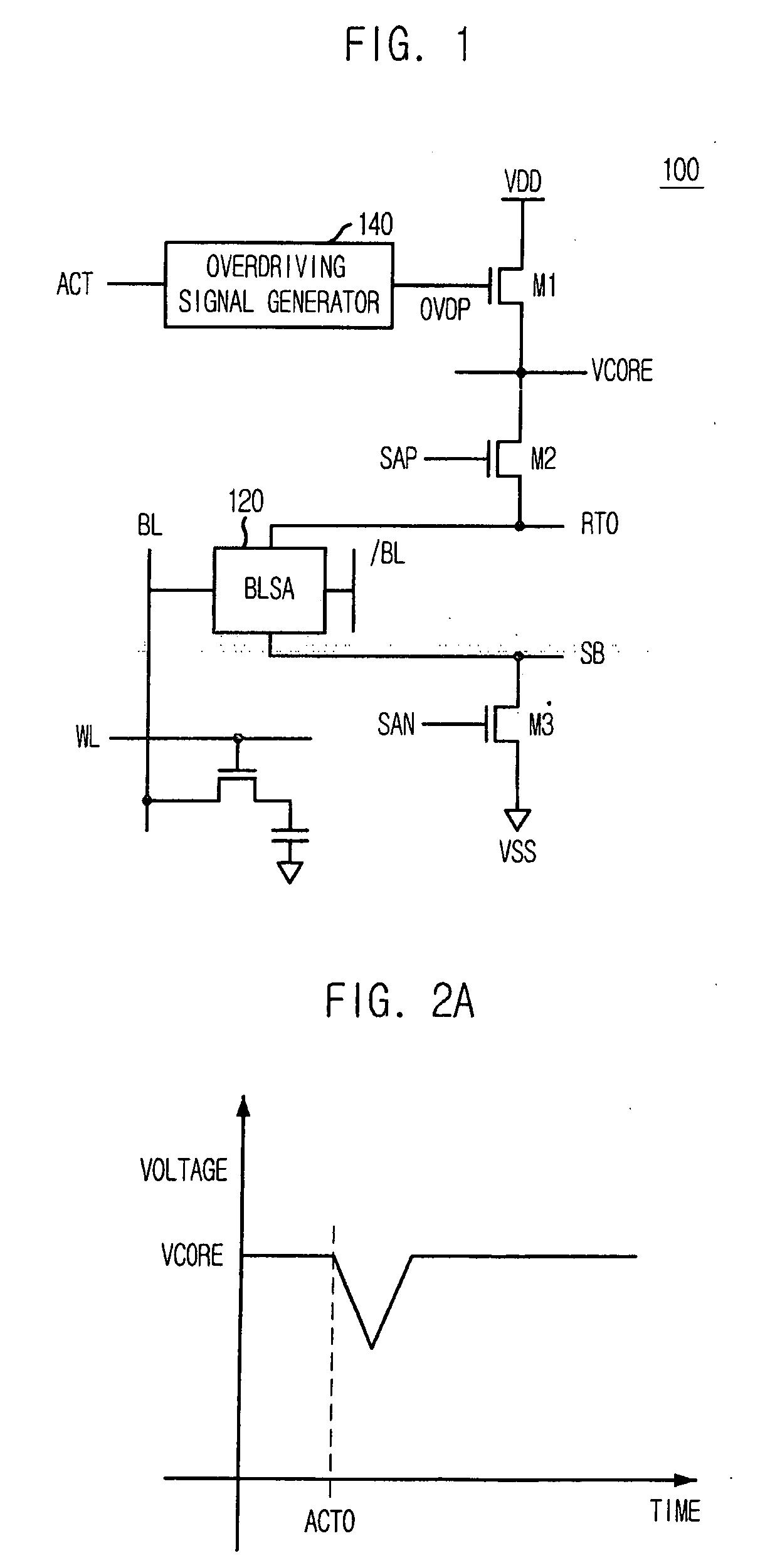
[0017]FIG. 1 is a schematic diagram of a BLSA control circuit in accordance with the present invention.

[0018] Referring to FIG. 1, the bit lines sense amplifier control circuit 100 includes a pull-up voltage line RT0 and a pull-down voltage line SB, each coupled to a BLSA 120. Also, the bit line sense amplifier includes a plurality of driver transistors M1, M2 and M3 for driving the voltage lines RT0 and SB to a specific voltage.

[0019] Specifically, a second driver transistor M2 drives the pull-up voltage line RT0 to a voltage of the VCORE terminal in response to a pull-up driving control signal SAP, and a third driver transistor M3 drives the pull-down voltage line SB to a ground voltage VSS in response to a pull-down driving control signal SAN. A first driver transistor M1 drives the VCORE terminal to an external voltage VDD in response to an overdriving signal OVDP.

[0020] An overdriving signal generator 140 generates the overdriving signal OVDP in response to an active command ...

second embodiment

[0029]FIG. 3 is a circuit diagram of a BLSA control circuit 200 for selectively outputting an overdriving signal in accordance with the present invention.

[0030] As shown, the BLSA control circuit 200 includes a BLSA 220, an overdriving signal generator 240, a plurality of driver transistors NM1, NM2 and NM3 and an overdriving control signal generator 400.

[0031] The overdriving signal generator 240 generates an overdriving signal OVDP in response to an active command ACT. The BLSA 220 is coupled between a pull-up voltage line RT0 and a pull-down voltage line SB. The plurality of driver transistors NM1, NM2 and NM3 drives the voltage lines RT0 and SB to a specific voltage. The overdriving control signal generator 400 selectively outputs the overdriving signal OVDP according to supply voltage circumstance, i.e., whether the supply voltage is a relatively high voltage or a relatively low voltage.

[0032] Specifically, a second driver transistor NM2 drives the pull-up voltage line RT0 to...


PUM


Abstract

A semiconductor memory device includes a bit line sense amplifier for sensing and amplifying data applied on a bit line; a first driver for driving a pull-up voltage line of the bit line sense amplifier to a voltage applied on a normal driving voltage terminal; an overdriving signal generator for generating an overdriving signal defining an overdriving period in response to an active command; an overdriving control signal generator for receiving the overdriving signal to generate an overdriving control signal for selectively performing an overdriving operation according to a voltage level of an overdriving voltage; and a second driver for driving the normal driving voltage terminal to the overdriving voltage in response to the overdriving control signal.

Description

FIELD OF THE INVENTION [0001] The present invention relates to a semiconductor memory device; and, more particularly, to a bit line, overdriving control circuit for use in a semiconductor memory device. DESCRIPTION OF RELATED ART [0002] As semiconductor memory chips are scaled down in line width and cell size, a power supply voltage becomes lower. Accordingly, there is a demand for semiconductor memory devices that can satisfy the low voltage requirement. [0003] Most of the semiconductor memory chips include internal voltage generators that generate a plurality of internal voltages from an external voltage. Thus, the semiconductor memory chips supply internal circuits with the internal voltages by themselves. In the memory devices such as DRAM using a bit line sense amplifier (BLSA), a core voltage VCORE corresponding to a voltage level of data “1” is used to detect cell data. [0004] When a word line selected by a row address is activated, data of a plurality of memory cells connect...

Claims


Application Information

Patent Timeline
IPC IPC(8): G11C11/34
CPCG11C5/145G11C7/06G11C11/4091G11C11/4074G11C7/12
Inventor KANG, KHIL-OHK
Owner SK HYNIX INC
Features
  • R&D
  • Intellectual Property
  • Life Sciences
  • Materials
  • Tech Scout
  • Unparalleled Data Quality
  • Higher Quality Content
  • 60% Fewer Hallucinations
Learn More