Vertical profile fixing

a technology of vertical profiles and fixing parts, applied in the field of semiconductor device formation, can solve problems such as irregular vertical profiles of mask features

Active Publication Date: 2007-04-05
LAM RES CORP
View PDF26 Cites 21 Cited by
  • Summary
  • Abstract
  • Description
  • Claims
  • Application Information

AI Technical Summary

Problems solved by technology

Such processes may cause mask feat...

Method used


Image

  • Vertical profile fixing
  • Vertical profile fixing
  • Vertical profile fixing

Examples


Embodiment Construction

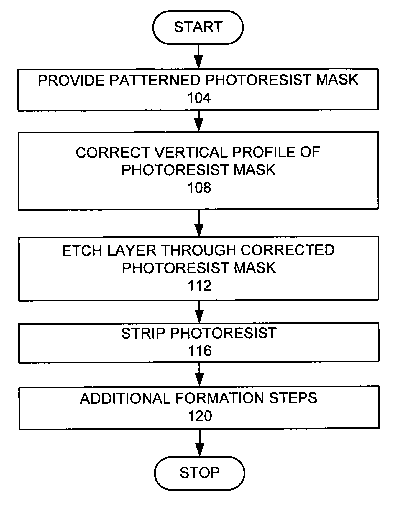
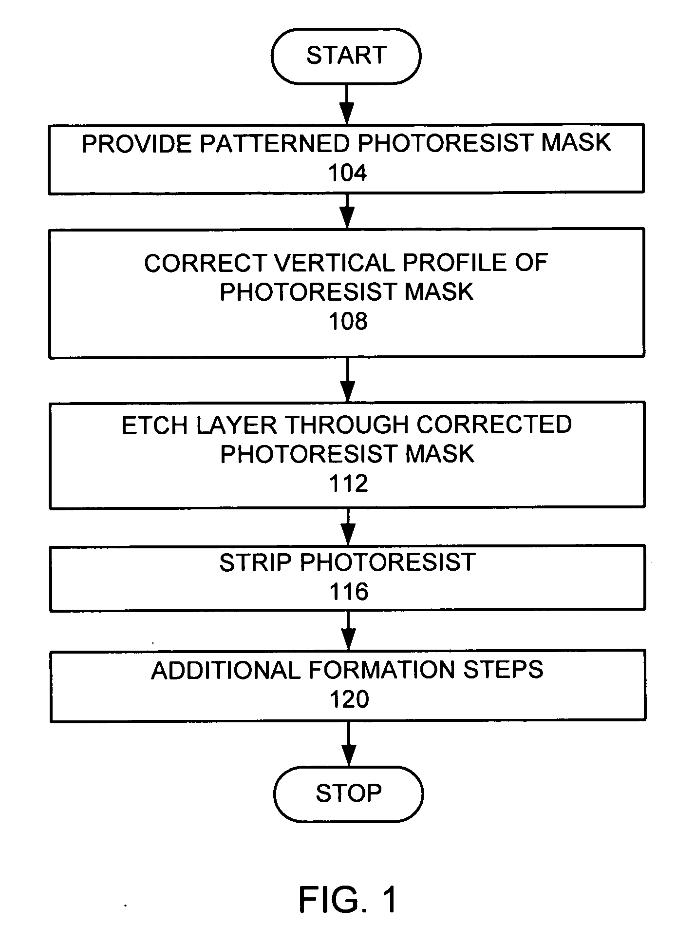
[0018] The present invention will now be described in detail with reference to a few preferred embodiments thereof as illustrated in the accompanying drawings. In the following description, numerous specific details are set forth in order to provide a thorough understanding of the present invention. It will be apparent, however, to one skilled in the art, that the present invention may be practiced without some or all of these specific details. In other instances, well known process steps and / or structures have not been described in detail in order to not unnecessarily obscure the present invention.

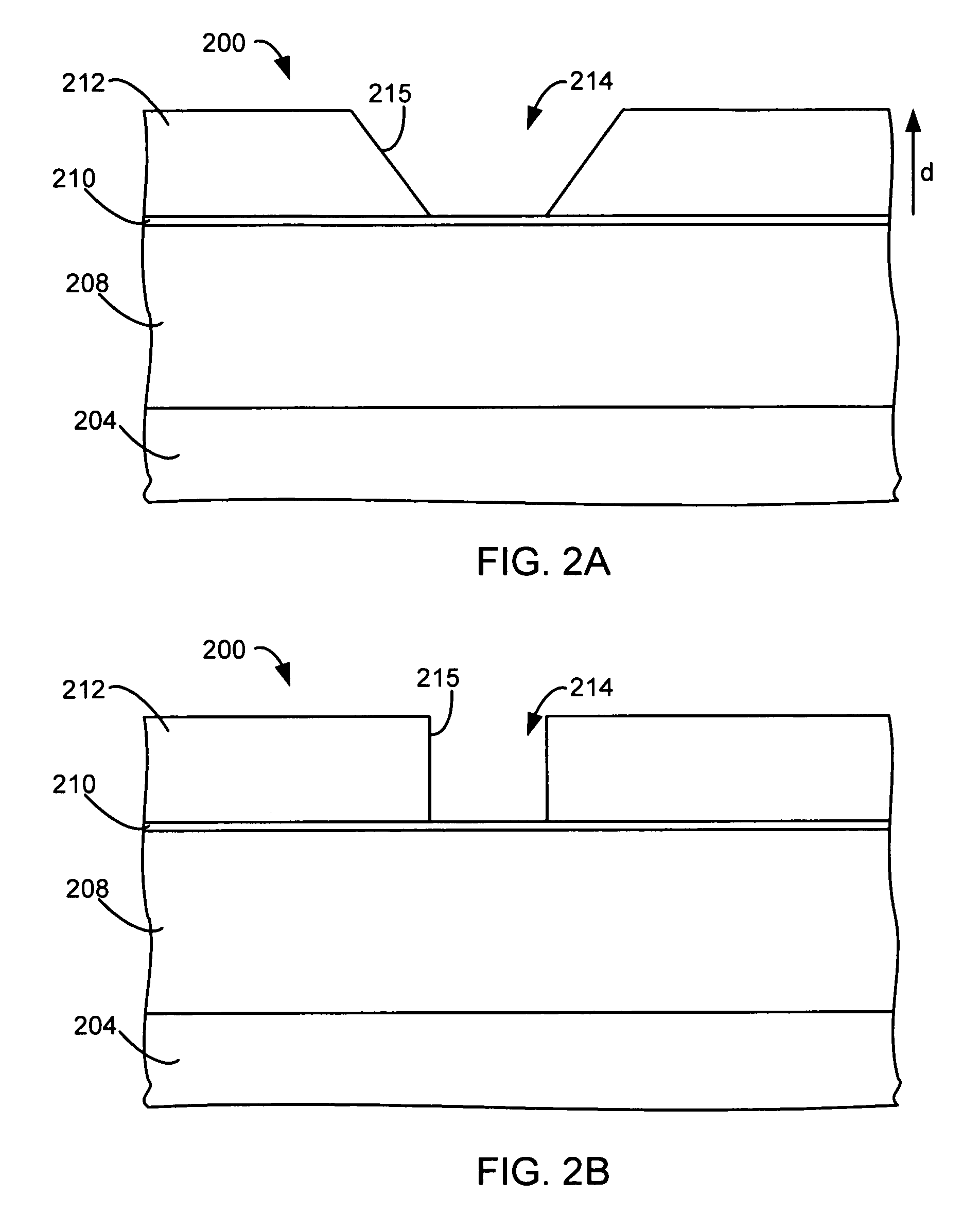
[0019] To facilitate understanding, FIG. 1 is a high level flow chart of a process that may be used in an embodiment of the invention. A patterned photoresist mask is provided (step 104). FIG. 2A is a schematic cross-sectional view of a layer to be etched 208 over a substrate 204, with a patterned photoresist mask 212 with a feature 214, over a ARL 210, over the etch layer 208 forming a ...


PUM

PropertyMeasurementUnit
Angleaaaaaaaaaa
Angleaaaaaaaaaa
Flow rateaaaaaaaaaa

Abstract

A method for etching features in an etch layer is provided. A patterned photoresist mask is formed over the etch layer with photoresist features with sidewalls wherein the sidewalls of the photoresist features have irregular profiles along depths of the photoresist features. The irregular profiles along the depths of the photoresist features of the sidewalls of the photoresist features are corrected comprising at least one cycle, where each cycle comprises a sidewall deposition phase and a profile shaping phase. Feature is etched into the etch layer through the photoresist features. The mask is removed.

Description

BACKGROUND OF THE INVENTION [0001] The present invention relates to the formation of semiconductor devices. [0002] During semiconductor wafer processing, features of the semiconductor device are defined in the wafer using well-known patterning and etching processes. In these processes, a photoresist (PR) material is deposited on the wafer and then is exposed to light filtered by a reticle. The reticle is generally a glass plate that is patterned with exemplary feature geometries that block light from propagating through the reticle. [0003] After passing through the reticle, the light contacts the surface of the photoresist material. The light changes the chemical composition of the photoresist material such that a developer can remove a portion of the photoresist material. In the case of positive photoresist materials, the exposed regions are removed, and in the case of negative photoresist materials, the unexposed regions are removed. Thereafter, the wafer is etched to remove the u...

Claims


Application Information

Patent Timeline
IPC IPC(8): B44C1/22C23F1/00H01L21/306C03C15/00
CPCH01L21/31144H01L21/0273G03F7/70475H01L21/3065
Inventor SADJADI, S.M. REZACIRIGLIANO, PETERKIM, JISOOHUANG, ZHISONGHUDSON, ERIC A.
Owner LAM RES CORP
Why Eureka
Try Eureka