High power light emitting diode package

a light-emitting diode and high-power technology, applied in the direction of light-emitting devices, semiconductor devices for light sources, solid-state devices, etc., can solve the problems of power loss, hindering heat dissipation, and degrading light efficiency as drawbacks, so as to improve heat dissipation efficiency, prevent light interference, and excellent light efficiency

Inactive Publication Date: 2007-04-05
SAMSUNG ELECTRO MECHANICS CO LTD
View PDF2 Cites 72 Cited by
  • Summary
  • Abstract
  • Description
  • Claims
  • Application Information

AI Technical Summary

Benefits of technology

[0032] That is, the dual reflector structure can preferably prevent light interference and raise heat dissipating efficiency with a lead frame having a group of indented recesses.
[0033] The present invention has been made to solve the foregoing problems of the prior art and therefore an object of certain embodiments of the present invention is to provide a high power LED package which has first reflectors arranged to correspond to a plurality of LED chips mounted on a single lead frame and a second reflector arr...

Problems solved by technology

Then, as shown in FIG. 4, lights emitted from adjacent ones of the LED chips 130, 230 interfere with each other, thereby degrading light efficiency as a drawback.
In addition, the high power LED package 100, 200 where several LED chips are mounted have some elements resistant against the LED chips 130, 230, which cause power loss...

Method used


Image

  • High power light emitting diode package
  • High power light emitting diode package
  • High power light emitting diode package

Examples


Embodiment Construction

[0058] The present invention will now be described more fully hereinafter with reference to the accompanying drawings, in which preferred embodiments of the invention are shown.

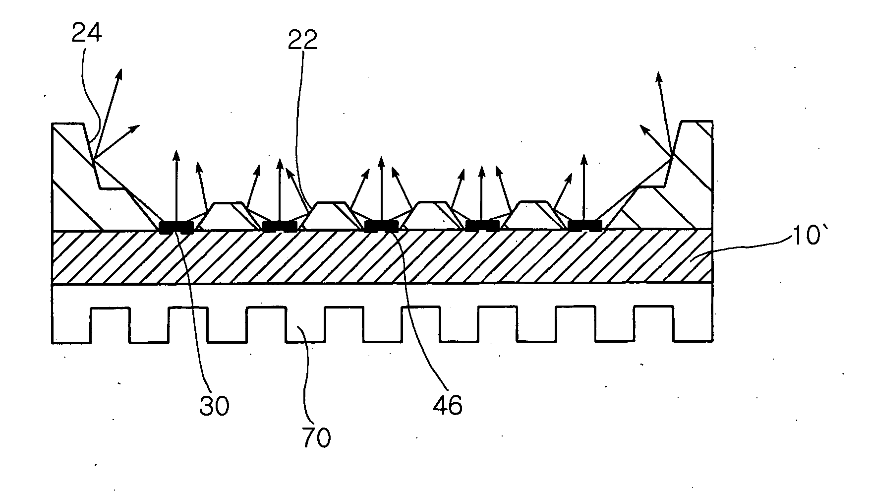
[0059] First, FIGS. 5 to 7 show a high power LED package 1 of the invention, in which FIG. 5 illustrates a lead frame or base member when LED chips are not mounted, FIG. 6 is a cross sectional view illustrating a high power LED package of the invention, and FIG. 7 illustrates important parts.

[0060] That is, as shown in FIGS. 6 and 7, the high power LED package 1 of the invention generally includes a base member 10, a reflector unit 20 provided on the base member 10, a plurality of LED chips 30 mounted on the base member 10 and surrounded at least by first reflectors 22 of the reflector unit 20 and a connection unit 40 arranged in the base member 10 to electrically connect the LED chips 30 to the outside.

[0061] In particular, as a technical feature, the reflector unit 20 also includes a second reflector 24 ...


PUM


Abstract

The invention relates to a high power LED package having excellent light efficiency and heat dissipating characteristics. The LED package includes a base member, a reflector unit arranged on the base member and having a plurality of first reflectors, a plurality of LED chips mounted on the base member and surrounded by the first reflectors, and a connection unit arranged on the base member, for electrically connecting the LED chips to an outside. The reflector unit also includes a second reflector surrounding the first reflectors. The second reflector is arranged to surround the first reflectors in order to completely prevent any interference of emission lights and collect the emission lights together, thereby enabling excellent light efficiency. Furthermore, with the first reflectors surrounding the individual LED chips, it is possible to maximize heat dissipating efficiency of the lead frame, thereby stabilizing operating characteristics of the package.

Description

CLAIM OF PRIORITY [0001] This application claims the benefit of Korean Patent Application No. 2005-93170 filed on Oct. 4, 2005, in the Korean Intellectual Property Office, the disclosure of which is incorporated herein by reference. BACKGROUND OF THE INVENTION [0002] 1. Field of the Invention [0003] The present invention relates to a high power Light Emitting Diode (LED) package, in particular, which is devised to receive a plurality of LED chips while preventing light interference to further enhance light efficiency, and in which a base member has recesses for seating the LED chips seated therein in order to ensure excellent heat dissipating ability. [0004] 2. Description of the Related Art [0005] LEDs are designed to emit light from excessive energy generating when applied electrons recombine with holes. Examples of such LEDs include a red LED based on GaAsP, a green LED based on GaP and a blue LED based on a double hetero structure of InGaN / AlGaN. [0006] The LEDs are widely used ...

Claims


Application Information

Patent Timeline
IPC IPC(8): H01L33/00H01L33/60H01L33/62H01L33/64
CPCF21K9/00H01L25/0753H01L33/60H01L33/64H01L33/642H01L2224/48091H01L2224/48137H01L2924/00014H01L2924/00F21K9/68
Inventor BAEK, JONG HWANPARK, JE MYUNGRYO, GEUN CHANGSEO, JUN HOPARK, JUNG KYU
Owner SAMSUNG ELECTRO MECHANICS CO LTD
Why Eureka
Try Eureka