Semiconductor device and a manufacturing method of the same
- Summary
- Abstract
- Description
- Claims
- Application Information
AI Technical Summary
Benefits of technology
Problems solved by technology
Method used
Image

Examples
embodiment 1
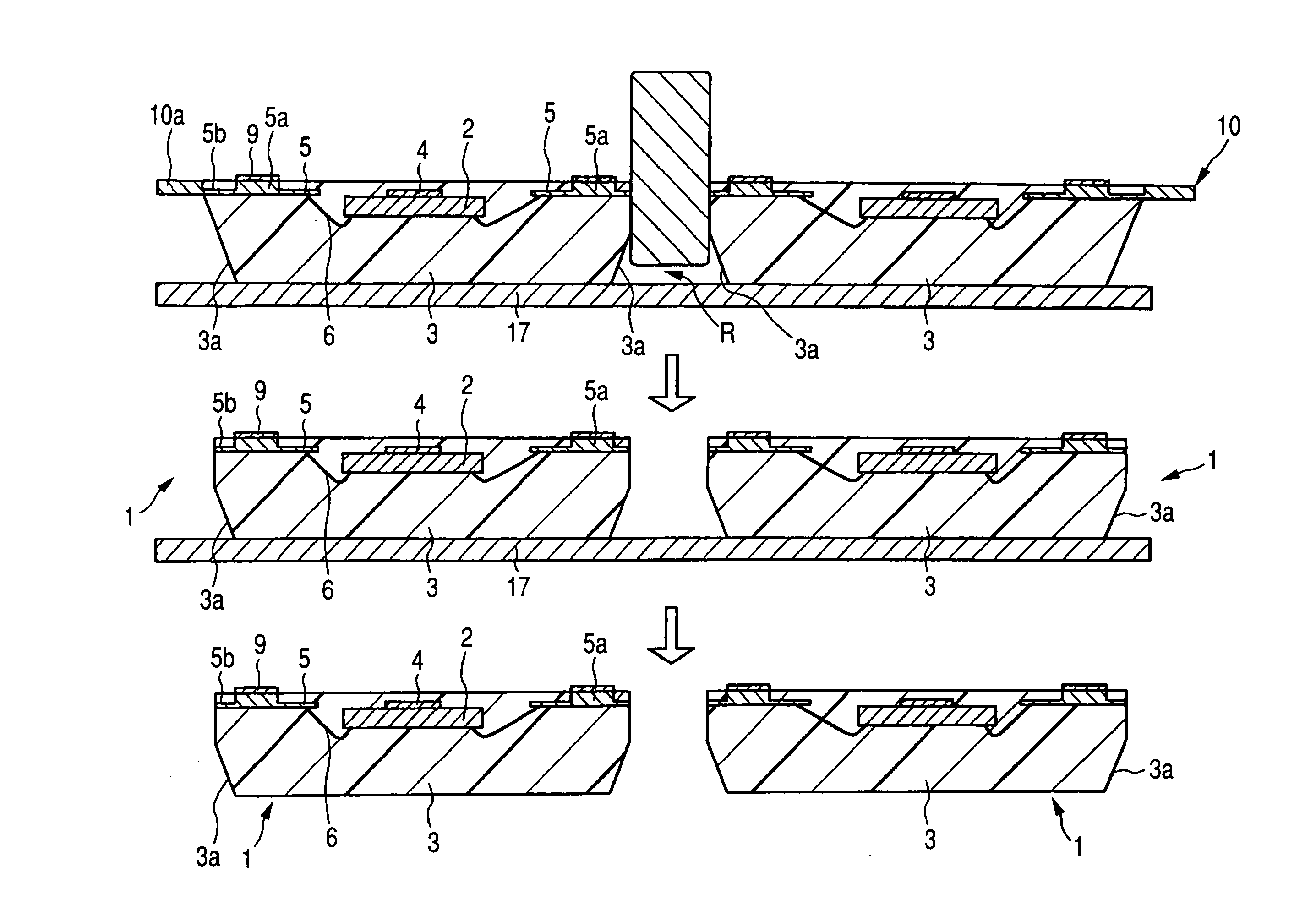
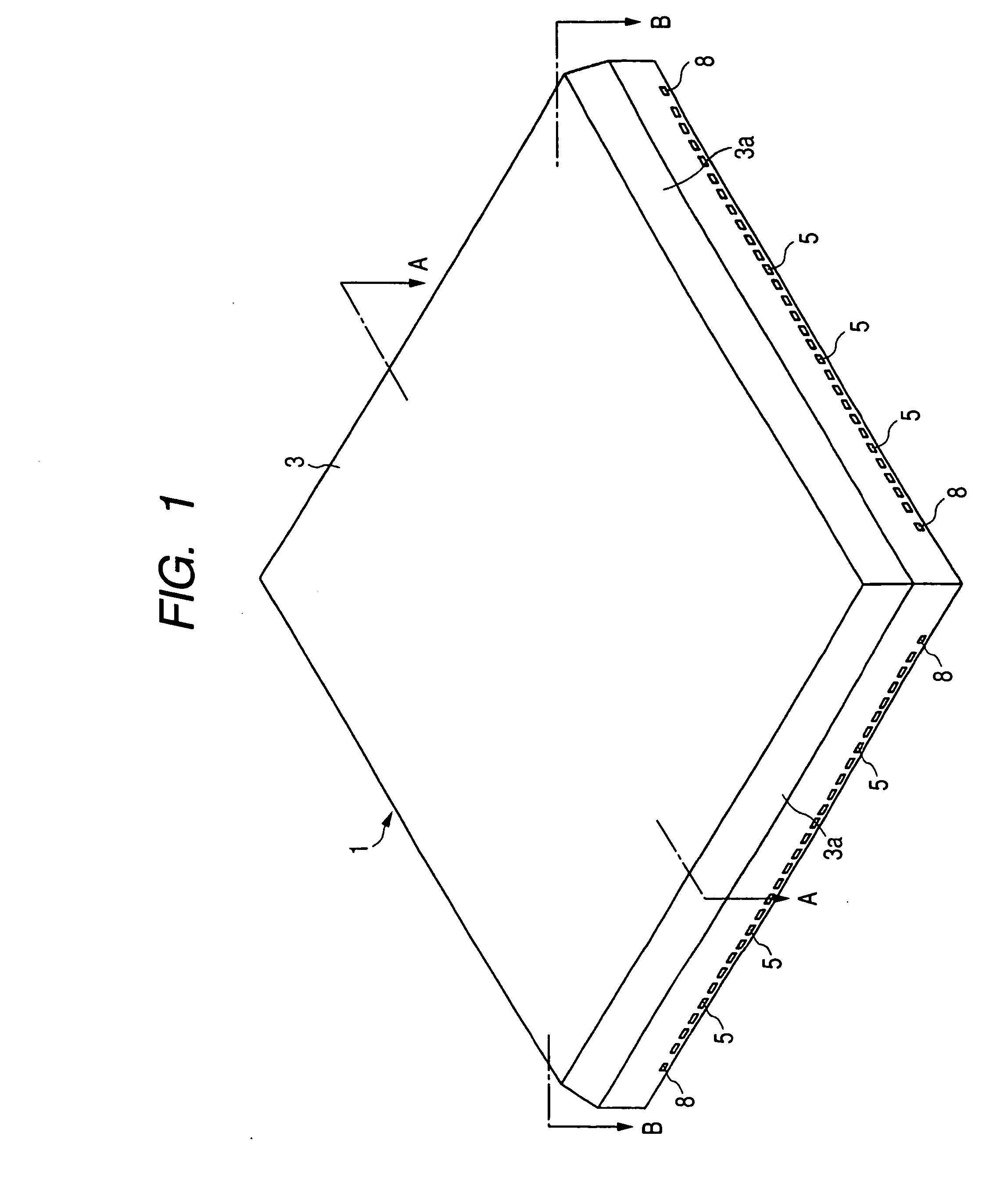
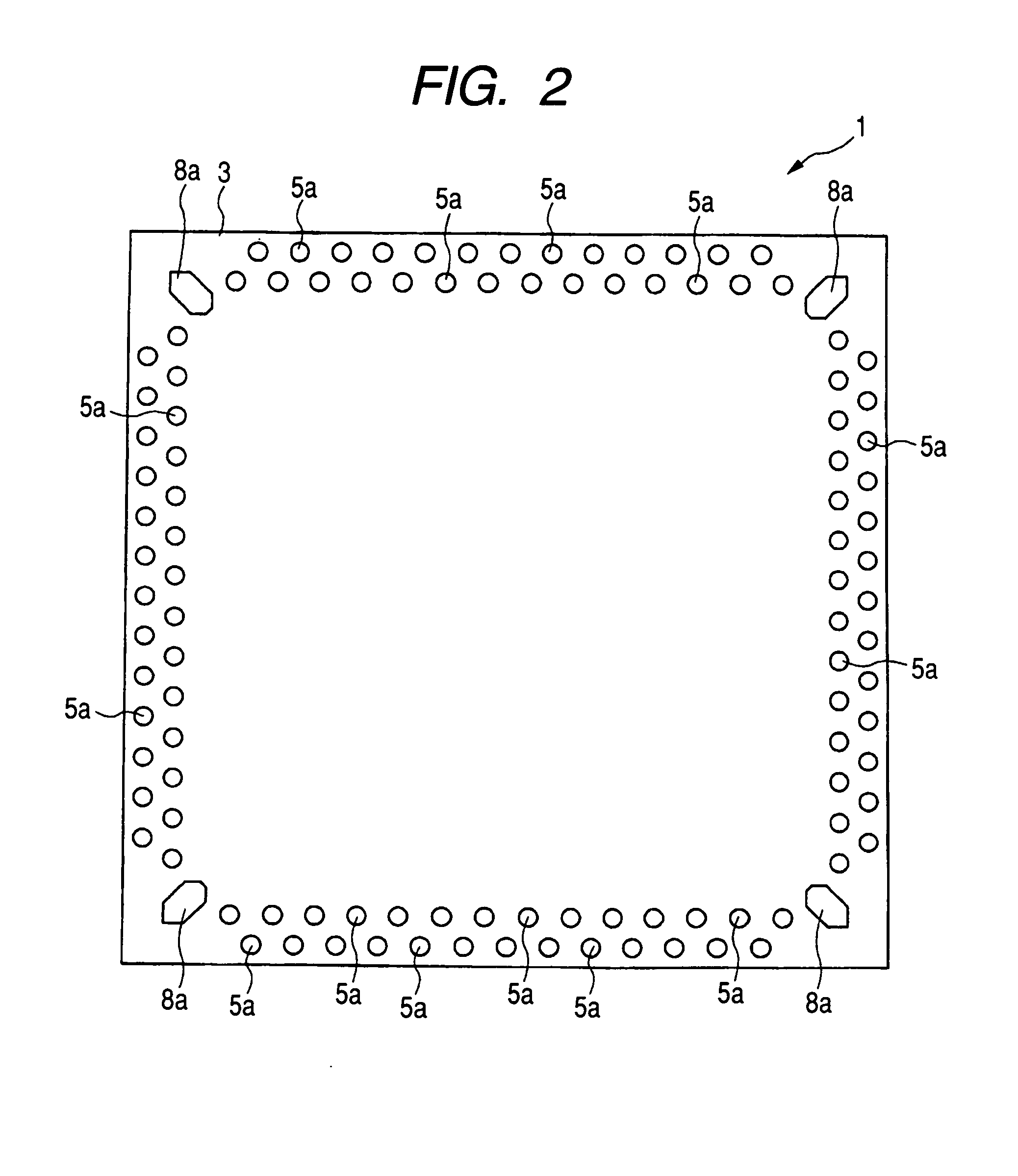
[0065]FIG. 1 is a perspective view showing an example of the structure of a semiconductor device of an embodiment 1 of the present invention, FIG. 2 is a back view showing the structure of the semiconductor device shown in FIG. 1, FIG. 3 is a cross-sectional view and an enlarged partial cross-sectional view showing the structure of across section taken along a line A-A shown in FIG. 1, FIG. 4 is a cross-sectional view and an enlarged partial cross-sectional view showing the structure of a cross section taken along a line B-B shown in FIG. 1. Further, FIG. 5 is a flow chart showing an example of assembling steps of the semiconductor device shown in FIG. 1, FIG. 6 is a cross-sectional view showing an example of the structure up to die bonding which is the assembling step shown in FIG. 5, FIG. 7 is a cross-sectional view showing an example of the structure up to resin molding which is the assembling step shown in FIG. 5, FIG. 8 is a cross-sectional view showing an example of the struct...
embodiment 2
[0117]FIG. 15 is a plan view showing an example of the internal structure of a semiconductor device according to an embodiment 2 of the present invention in a state that the inner structure is viewed through the sealing body in a see-through manner, FIG. 16 is a cross-sectional view showing the structure of a cross section taken along a line A-A shown in FIG. 15, FIG. 17 is a plan view showing the structure of the semiconductor device shown in FIG. 15, FIG. 18 is a back view showing the structure of the semiconductor device shown in FIG. 15, FIG. 19 is a back view showing the internal structure of a back side of a chip of the semiconductor device shown in FIG. 15, FIG. 20 is a plan view showing an example of the structure when a dicing tape is adhered in an assembling step of the semiconductor device shown in FIG. 15, FIG. 21 is a plan view showing an example of the structure after a sealing body is cut into individual pieces in the assembling step of the semiconductor device shown ...
PUM
 Abstract
Description
Claims
Application Information
 - R&D Engineer
- R&D Manager
- IP Professional
- Industry Leading Data Capabilities
- Powerful AI technology
- Patent DNA Extraction
Browse by: Latest US Patents, China's latest patents, Technical Efficacy Thesaurus, Application Domain, Technology Topic.
© 2024 PatSnap. All rights reserved.Legal|Privacy policy|Modern Slavery Act Transparency Statement|Sitemap