Housing for an electromagnetic radiation emitting optoelectronic component, component and method of making a housing or a component
- Summary
- Abstract
- Description
- Claims
- Application Information
AI Technical Summary
Benefits of technology
Problems solved by technology
Method used
Image

Examples
Embodiment Construction
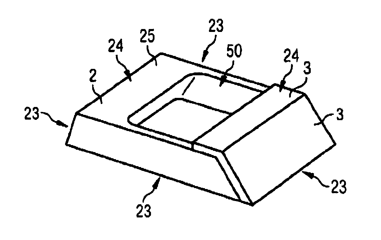
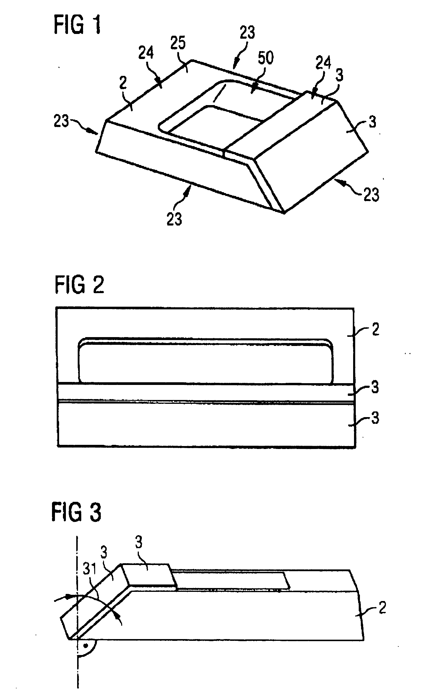
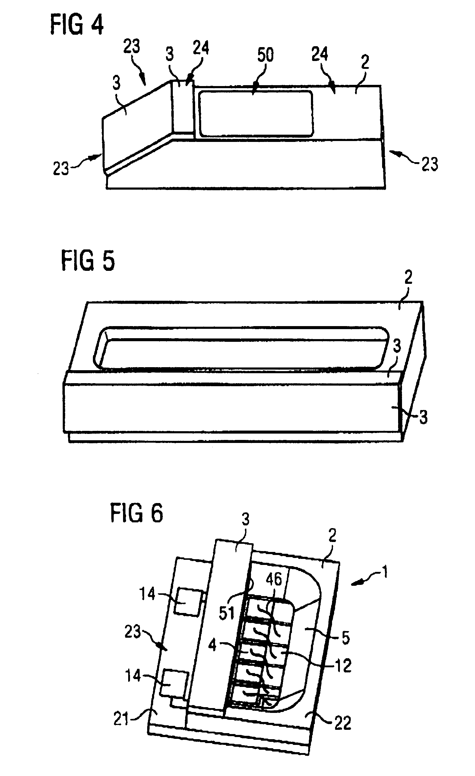
[0041] In the exemplary embodiments and figures, like or like-acting elements are provided with the same respective reference numerals. The elements shown and the size relationships of the elements to one another are not necessarily to be considered true to scale. Rather, individual details of the figures may be depicted as exaggeratedly large to provide a better understanding. This is true in particular of the exemplary depictions of the baffle layer.
[0042] The housing 2 illustrated in FIGS. 1 to 3 comprises a housing body 25 provided with a cavity 50. The opening of the cavity 50 has an elongated cross-sectional area, configured for example in the manner of a rectangle with rounded edges. The cavity 50 is provided to have at least one luminescent diode chip mounted in it and to be electrically conductively connected. The housing illustrated in FIGS. 1 to 3 is provided for example to accommodate four or five luminescent diode chips, which are mounted, for example in a linear arran...
PUM
 Abstract
Description
Claims
Application Information
 - R&D Engineer
- R&D Manager
- IP Professional
- Industry Leading Data Capabilities
- Powerful AI technology
- Patent DNA Extraction
Browse by: Latest US Patents, China's latest patents, Technical Efficacy Thesaurus, Application Domain, Technology Topic.
© 2024 PatSnap. All rights reserved.Legal|Privacy policy|Modern Slavery Act Transparency Statement|Sitemap