Electronic component testing apparatus and method for electronic component testing

a technology for electronic components and test apparatuses, applied in the direction of individual semiconductor device testing, packaging goods type, instruments, etc., can solve the problems of b>1/b> percent or more of ics to fail, and damage to the integrated circuit (ics), etc., to achieve the effect of increasing the yield

Inactive Publication Date: 2007-05-17
KING YUAN ELECTRONICS
View PDF14 Cites 0 Cited by
  • Summary
  • Abstract
  • Description
  • Claims
  • Application Information

AI Technical Summary

Benefits of technology

[0012] In view of the foregoing, it is an object of the present invention to provide a test apparatus and a test method for decreasing the probability of tested component stayed in the test area when the final test has finished, and therefore increasing the yield.

Problems solved by technology

During the packaging process, Integrated circuit (ICs) may be damaged or packaging may not be correctly performed.
The failures introduced during packaging typically cause 1 percent or more of ICs to fail.
The long tact time cause the yield decreases significantly.
Moreover, if the test time of the IC is shorter, then the time during wait will get longer.
The modern semiconductor production test equipment is increasingly complex to design, build and maintain.

Method used


Image

  • Electronic component testing apparatus and method for electronic component testing
  • Electronic component testing apparatus and method for electronic component testing
  • Electronic component testing apparatus and method for electronic component testing

Examples


Embodiment Construction

[0020] The detailed description of the present invention will be discussed in the following embodiment, which is not intended to limit the scope of the present invention, but can be adapted for other applications. While drawings are illustrated in details, it is appreciated that the quantity of the disclosed components may be greater or less than that disclosed, except expressly restricting the amount of the components.

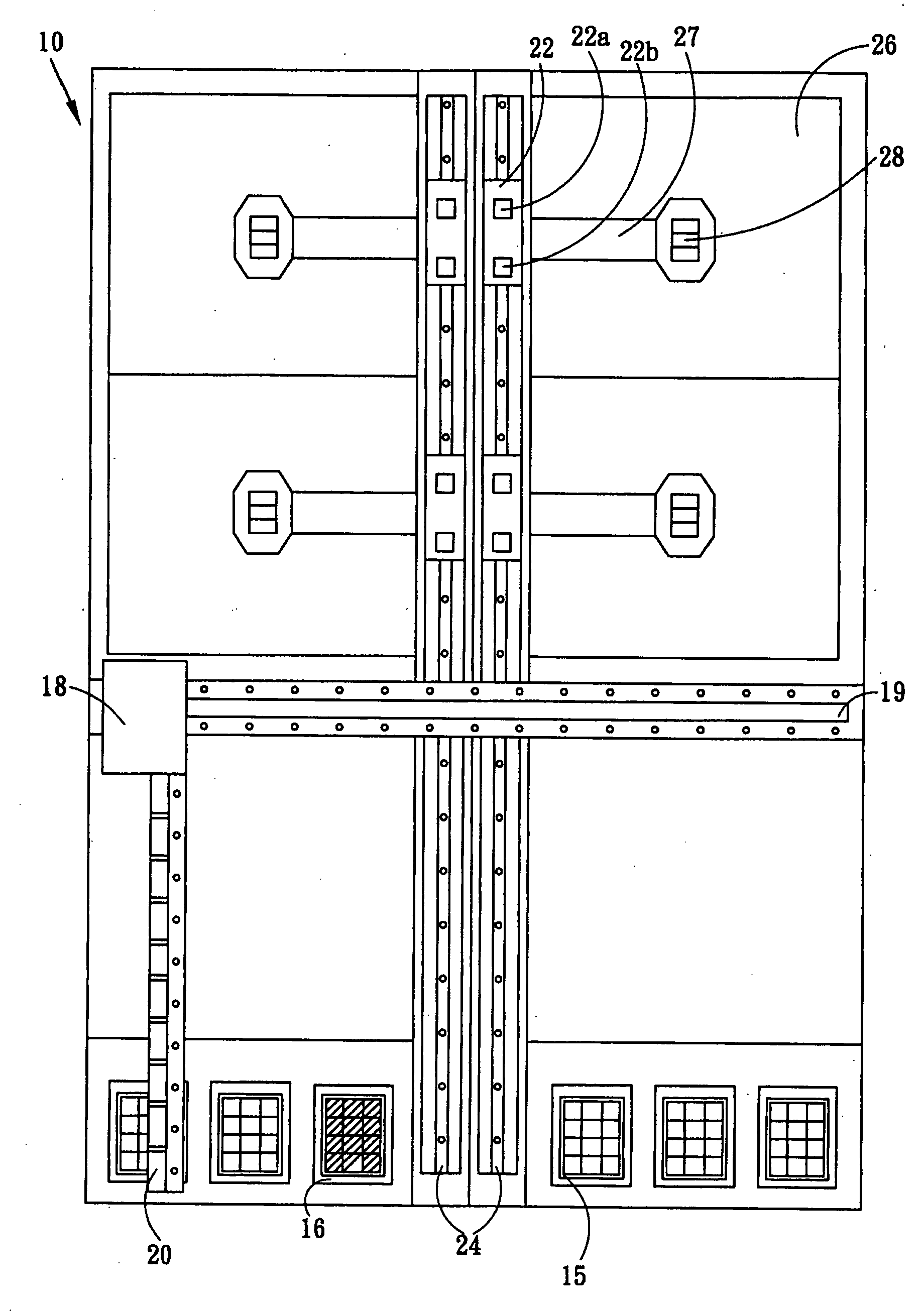
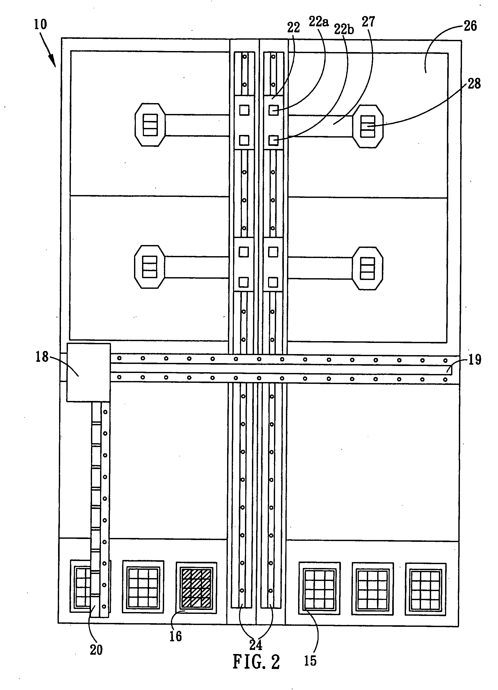
[0021]FIG. 2 shows the vertical plan view of ICs test apparatus according to one embodiment of the present invention. Pluralities of input trays 16 for storing the ICs are stacking arrangements in the input / output zone of the handler 10. Each of the input trays 16 with a plurality of IC aligned thereon. Similar to input trays 16, there is also at least one output tray 15 located within the input / output zone for storing the tested IC. The tested ICs are graded to output trays 15 according to measured parameter. The number of input / output trays 16 / 15 and their location...


PUM


Abstract

The present invention discloses an electronic testing apparatus and a continuous test method for electronic component, which includes multiple test areas, each area possesses respective pick and place module. The apparatus includes multiple shuttles located between the test area and input / output trays. Moreover, a further pick and place module is utilized, between the shuttles and the input / output trays, for picking and placing the devices under test or tested device. The method delivers different electronic component to different test area for testing by different shuttles and to perform testing continuously.

Description

CROSS REFERENCE [0001] This application is a continuation-in-part of U.S. patent application Ser. No. 11 / 233,589, filed Sep. 22, 2005.BACKGROUND OF THE INVENTION [0002] 1. Field of the Invention [0003] The present invention generally relates to an electronic component test device and the method for electronic component testing, and more particularly to an Integrated Circuit (ICs) test device and the method for ICs testing, which includes a plurality of shuttles having individual pick and place module. [0004] 2. Description of the Prior Art [0005] During the packaging process, Integrated circuit (ICs) may be damaged or packaging may not be correctly performed. The failures introduced during packaging typically cause 1 percent or more of ICs to fail. Therefore it is necessary to perform the final test, which fully inspection performed on each packaged IC prior to shipment, in order to satisfy customer's requirement. [0006]FIG. 1 shows the vertical plan view of conventional test appara...

Claims


Application Information

Patent Timeline
Patent Type & Authority Applications(United States)
IPC IPC(8): G01R31/26
CPCG01R31/2893
Inventor CHIH-HUBG, HSIEH
Owner KING YUAN ELECTRONICS
Why Eureka
Try Eureka