Ultra-thin quad flat no-lead (QFN) package

a flat no-lead, ultra-thin technology, applied in the direction of basic electric elements, solid-state devices, electric devices, etc., can solve the problems of leadframe design, warpage, variation, delamination,

Active Publication Date: 2007-05-24
STMICROELECTRONICS ASIA PACIFIC PTE
View PDF6 Cites 32 Cited by
  • Summary
  • Abstract
  • Description
  • Claims
  • Application Information

AI Technical Summary

Problems solved by technology

However, the exposed contact areas of the leads on the top and bottom package surfaces are not aligned in the package thickness direction due to one-sided recesses formed in the leads.
This leadframe design has certain disadvantages such as warpage, variation, and delamination.
Furthermore, the disclosed internal package lacks versatility of stacking two or more packages or stacking one package in two different directions.
The reason for why the contact areas of the leads are offset may be due to the limitation of the method used to manufacture the leadframe.
Among them are thick package with a total package height over 1.5 mm, high tooling cost for requiring dedicated cavity mold for different sized OQFN packages, material cost for glass lid and attach, and additional process steps of glass lid attach.

Method used


Image

  • Ultra-thin quad flat no-lead (QFN) package
  • Ultra-thin quad flat no-lead (QFN) package
  • Ultra-thin quad flat no-lead (QFN) package

Examples


Embodiment Construction

[0025] Throughout this application, where publications are referenced, the disclosures of these publications are hereby incorporated by reference, in their entireties, into this application in order to more fully describe the state of art to which this disclosure pertains.

[0026] The present disclosure provides an ultra-thin Quad Flat No-Lead (QFN) semiconductor chip package, an ultra-thin Optical Quad Flat No-Lead (OQFN) semiconductor chip package, and methods of manufacturing the packages. The following description will omit details of materials and process techniques that are known to those skilled in the art. The omissions is are for the sake of brevity and no obscurity of do not obscure the principles or the implementations of the present disclosure.

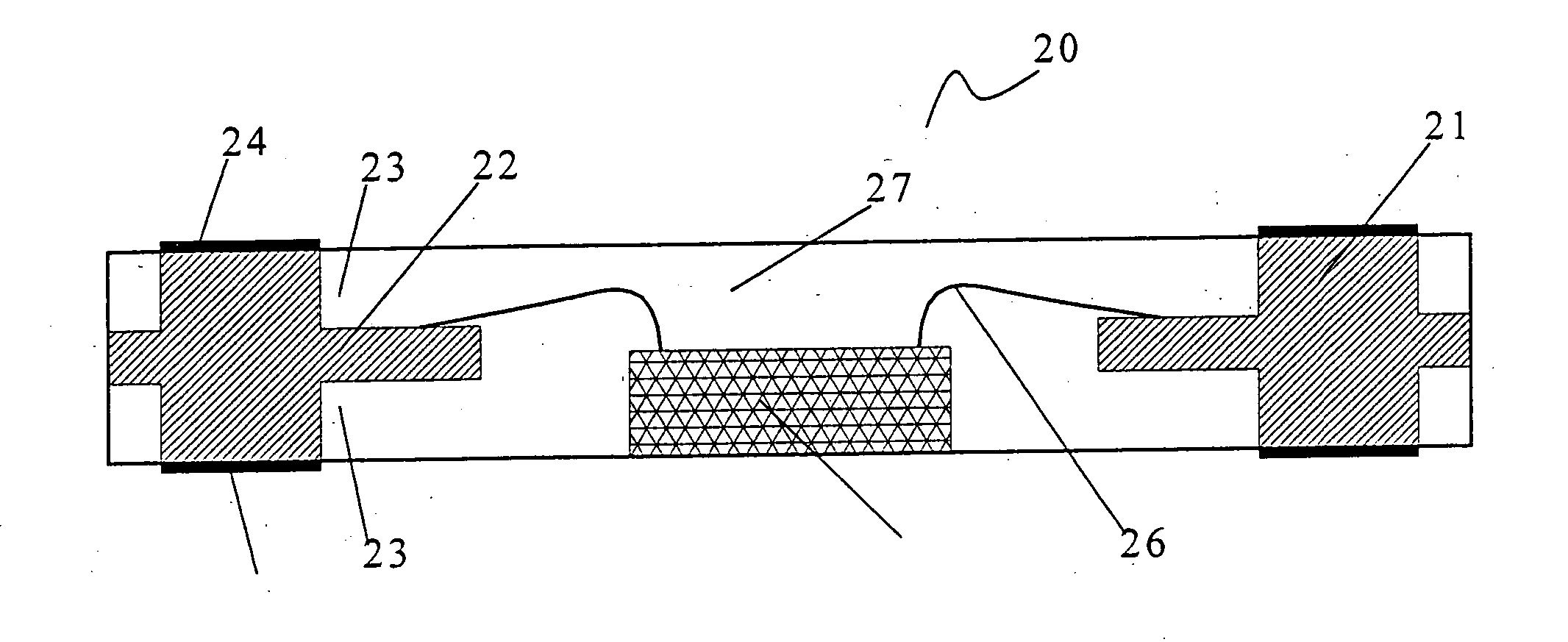
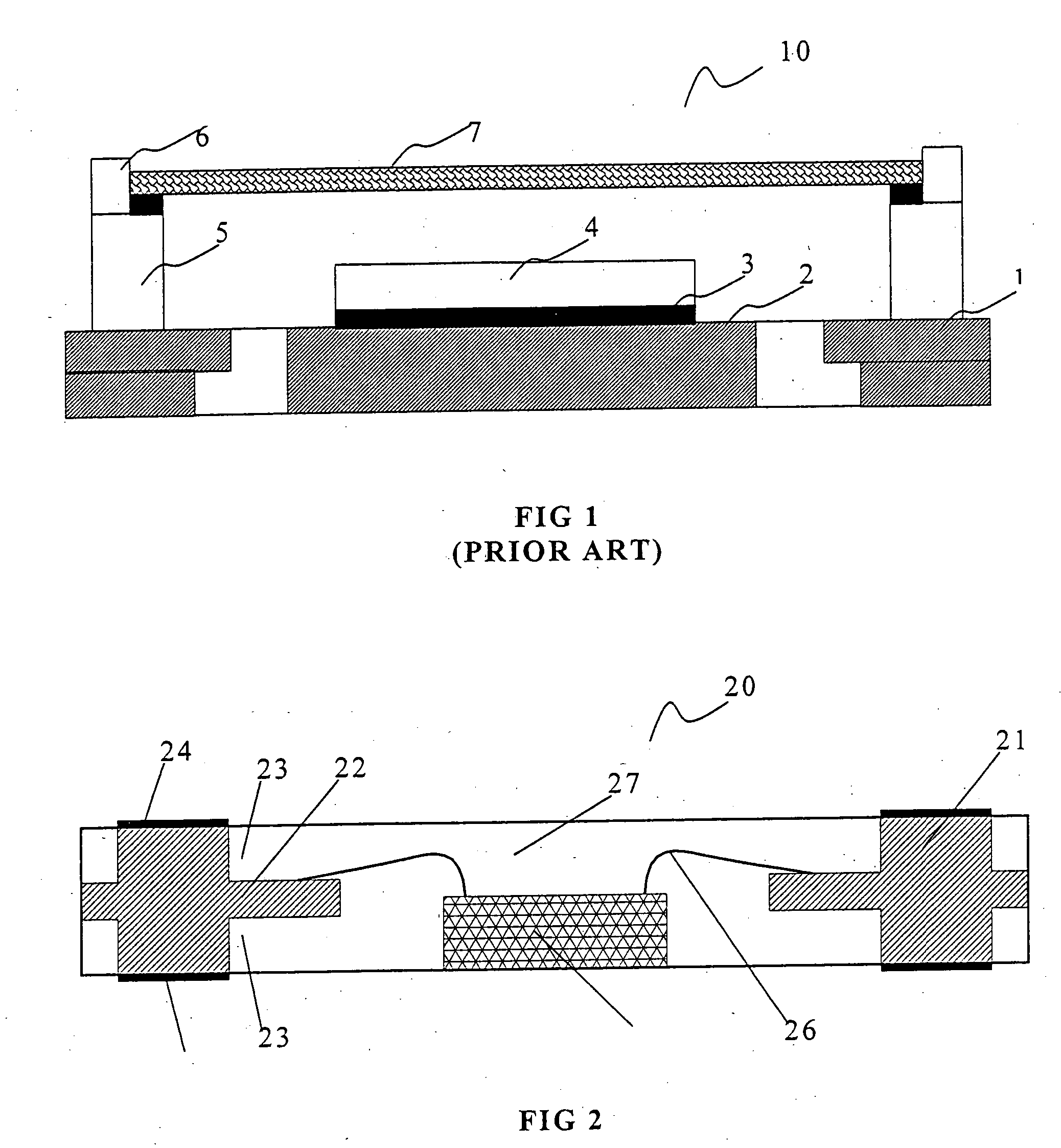
[0027]FIG. 2, is a simplified cross-sectional view of the QFN package according to one embodiment of the present disclosure. The QFN package 20 includes a leadframe 21, a die 25, and a molding compound 27. The leadframe 21 has a to...


PUM


Abstract

An ultra-thin Quad Flat No-Lead (QFN) semiconductor chip package having a leadframe with lead terminals formed by recesses from both the top and bottom surfaces and substantially aligned contact areas formed on either the top or bottom surfaces. A die is electrically connected to the plurality of lead terminals and a molding compound encapsulates the leadframe and die together so as to form the ultra-thin QFN package. Accordingly, the substantially aligned contact areas are exposed on both the top and bottom surfaces of the package. The present disclosure also provides an ultra-thin Optical Quad Flat No-Lead (OQFN) semiconductor chip package, a stacked semiconductor module comprising at least two QFN semiconductor chip packages, and a method for manufacturing an ultra-thin Quad Flat No-Lead (QFN) semiconductor packages.

Description

CROSS-REFERENCE TO RELATED APPLICATIONS [0001] This patent application claims priority under 35 U.S.C. § 119(a) to Singapore Patent Application No. 200507285-5 entitled “ULTRA-THIN QUAD FLAT NO-LEAD (QFN) PACKAGE AND METHOD OF FABRICATING THE SAME” filed on Nov. 21, 2005, which is hereby incorporated by reference. TECHNICAL FIELD [0002] The present disclosure generally relates to semiconductor chip packages and packaging technologies, and more particularly to an ultra-thin quad flat no-lead package and method of fabricating the package. BACKGROUND [0003] Quad Flat No-lead (QFN) semiconductor chip packaging technology provides compact and reliable chip packages. The size of a semiconductor chip package, especially the height, is important in increasing the density of semiconductor chips in an electronic device. For example, conventional methods disclose a semiconductor package that comprises an external leadless leadframe package and an internal package, wherein the internal package ...

Claims


Application Information

Patent Timeline
Patent Type & Authority Applications(United States)
IPC IPC(8): H01L23/495
CPCH01L21/561H01L21/568H01L23/3107H01L23/49548H01L24/97H01L25/105H01L2224/16245H01L2224/48091H01L2224/48247H01L2224/97H01L2924/01029H01L2924/01078H01L2924/01082H01L2924/18165H01L2224/85H01L2924/00014H01L24/48H01L2924/01006H01L2924/01033H01L2924/014H01L2924/3511H01L2225/1029H01L2225/1058H01L2924/14H01L2924/181H01L2924/00H01L2924/00012H01L2224/45099H01L2224/45015H01L2924/207
Inventor GOH, KIM-YONGTEE, TONG-YAN
Owner STMICROELECTRONICS ASIA PACIFIC PTE
Why Eureka
Try Eureka