Fixed abrasive polishing pad, method of preparing the same, and chemical mechanical polishing apparatus including the same

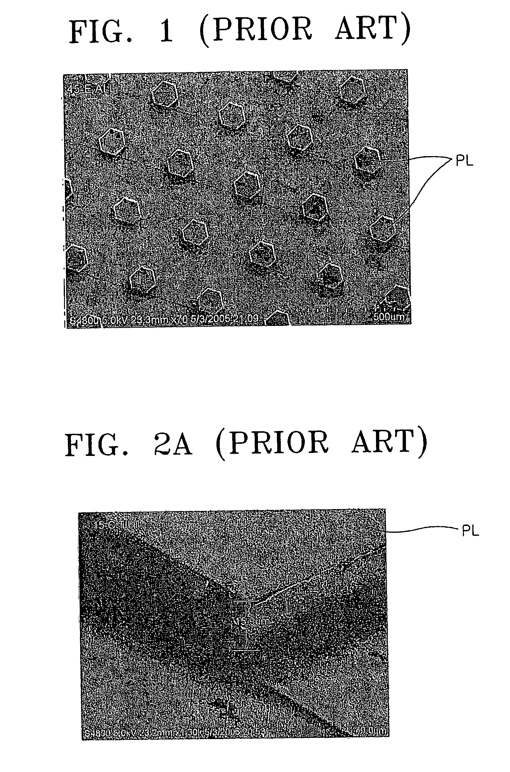
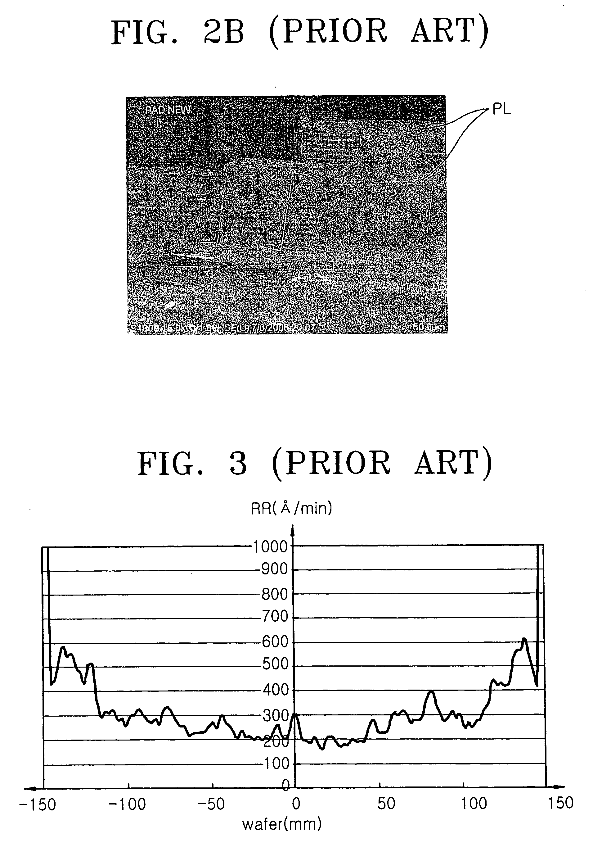
a technology of fixed abrasives and polishing pads, which is applied in the direction of gear teeth, manufacturing tools, gear teeth, etc., can solve the problems of difficult to increase the contact pressure between the polishing pads and the wafer, increase the etch rate of oxide film across the wafer, and ineffective removal of the nitride film at the center of the wafer, etc., to achieve the effect of enhancing the ability of a slurry to infiltrate a contact area

Inactive Publication Date: 2007-06-07
SAMSUNG ELECTRONICS CO LTD
View PDF24 Cites 86 Cited by
  • Summary
  • Abstract
  • Description
  • Claims
  • Application Information

AI Technical Summary

Benefits of technology

[0013] It is therefore another feature of an embodiment of the present invention to provide a polishing pad having polishing layers with apertu

Problems solved by technology

As a result, the oxide film overlying the nitride film at the center of the wafer is not effectively removed.
However, it may be difficult to increase the contact pressure between the polishing pad and the wafer only at the center of the wafer because of the characteristics of the polishing pad, and thus the oxide film etch rate may increase across the wafer.
Besides being difficult to apply more p

Method used


Image

  • Fixed abrasive polishing pad, method of preparing the same, and chemical mechanical polishing apparatus including the same
  • Fixed abrasive polishing pad, method of preparing the same, and chemical mechanical polishing apparatus including the same
  • Fixed abrasive polishing pad, method of preparing the same, and chemical mechanical polishing apparatus including the same

Examples


Embodiment Construction

[0032] Korean Patent Application Nos. 10-2005-0119089 and 10-2006-0047120, filed on Dec. 7, 2005, and May 25, 2006, respectively, in the Korean Intellectual Property Office, both of which are entitled “Fixed Abrasive Polishing Pad, Method of Preparing the Same, and Chemical Mechanical Polishing Apparatus Including the Same,” are incorporated by reference herein in their entirety.

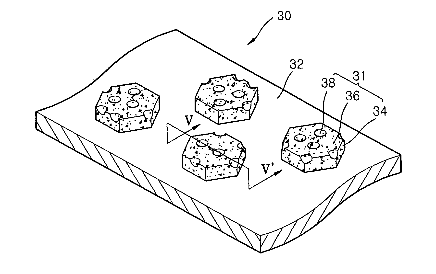
[0033] The present invention will now be described more fully hereinafter with reference to the accompanying drawings, in which exemplary embodiments of the invention are illustrated. The invention may, however, be embodied in different forms and should not be construed as limited to the embodiments set forth herein. Rather, these embodiments are provided so that this disclosure will be thorough and complete, and will fully convey the scope of the invention to those skilled in the art.

[0034] In the figures, the dimensions of layers and regions may be exaggerated for clarity of illustration. It will also be...


PUM

PropertyMeasurementUnit
Fractionaaaaaaaaaa
Fractionaaaaaaaaaa
Areaaaaaaaaaaa

Abstract

A fixed abrasive polishing pad includes a base and a plurality of polishing layers on the base, wherein each polishing layer includes abrasive particles and apertures in a polishing surface of the polishing layer.

Description

BACKGROUND OF THE INVENTION [0001] 1. Field of the Invention [0002] The present invention relates to an apparatus for manufacturing a semiconductor device. More particularly, the present invention relates to a fixed abrasive polishing pad, a method of preparing the same, and chemical mechanical polishing (CMP) apparatus including the same. [0003] 2. Description of the Related Art [0004] CMP is a process for planarizing a surface of a substrate, e.g., a semiconductor wafer, which may include a variety of structures, films, etc. formed thereon. CMP effects planarization by combining a mechanical polishing effect with a chemical reaction effect. The mechanical polishing typically involves the application of an abrasive to the wafer surface. The chemical reaction typically involves the application of a reactant solution, e.g., an acidic or basic solution, to the wafer. CMP is a planarization process frequently employed for removing protrusions from a wafer surface, and is very important...

Claims


Application Information

Patent Timeline
IPC IPC(8): B24B1/00B24B29/00
CPCB24B37/245B24B37/26
Inventor YOON, IL-YOUNGSHIN, HONG-JAELEE, SE-YOUNGCHOO, JAE-OUKKOO, JA-EUNG
Owner SAMSUNG ELECTRONICS CO LTD
Why Eureka
Try Eureka