

Organic semiconductor material and organic electronic device
a technology of organic semiconductors and electronic devices, applied in the direction of organic chemistry, solid-state devices, thermoelectric devices, etc., can solve the problems of inadequate mobility and achieve the effects of excellent flexibility, light weight and scarce breakability
- Summary
- Abstract
- Description
- Claims
- Application Information
AI Technical Summary
Problems solved by technology
Method used
Image

Examples
preparation example 2
[0185] 0.02 g of the bicyclo compound (1) of Preparation Example 1 and 0.1 g of zinc acetate dihydrate were put in a solvent mixture comprising 30 ml of chloroform and 3 ml of methanol, followed by stirring at room temperature for 3 hours. The reaction solution was washed twice with 100 ml of water and once with 40 ml of a saturated sodium chloride aqueous solution. The organic phase was dried over sodium sulfate. The solvent was distilled off, and the obtained solid was recrystallized from a solvent mixture of chloroform and methanol to obtain 0.022 g of a zinc complex of the bicyclo compound (1). Further, by gel permeation chromatography (Nippon Bunseki Kogyo JAIGEL-1H, 2H, chloroform), only the single peak was fractionated and purified.
[0186] The mass spectrum was measured, and the molecular peak was confirmed.
PREPRATION EXAMPLE 3
Preparation of 21, 23-dithiaporphyrin 5
[0187] A dithiaporphyrin compound having the following bicyclo ring structure was prepared by the following s...
preparation example 4
Preparation of 21-thiaporphyrin
[0197] In the same manner as in Preparation Example 3, thiatripyran dicarboxylic acid 4 was prepared. In the same manner as in Preparation Example 3 except that this thiatripyran dicarboxylic acid 4 and a pyrrole derivative instead of thiophene were employed, a thiaporphyrin compound having the following bicyclo structure was prepared by the following synthesis route.
[0198] Into a light-shielded 500 ml flask, thiatripyran dicarboxylic acid 4 (0.508 g, 0.9 mmol) was put, and after flushing the interior with argon, 2.5 ml of TFA was put at room temperature, followed by stirring for 5 minutes. 200 ml of dry CH2Cl2 was added, and then, diformylpyrrole (0.181 g, 0.9 mmol) was quickly added, followed by stirring at room temperature for 16 hours. Then, triethylamine was slowly added to neutralize the solution, and then DDQ (0.227 g, 1.0 mmol) was added, followed by stirring for further 2 hours. The obtained solution was washed with water, a saturated sodiu...
example 1
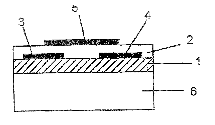
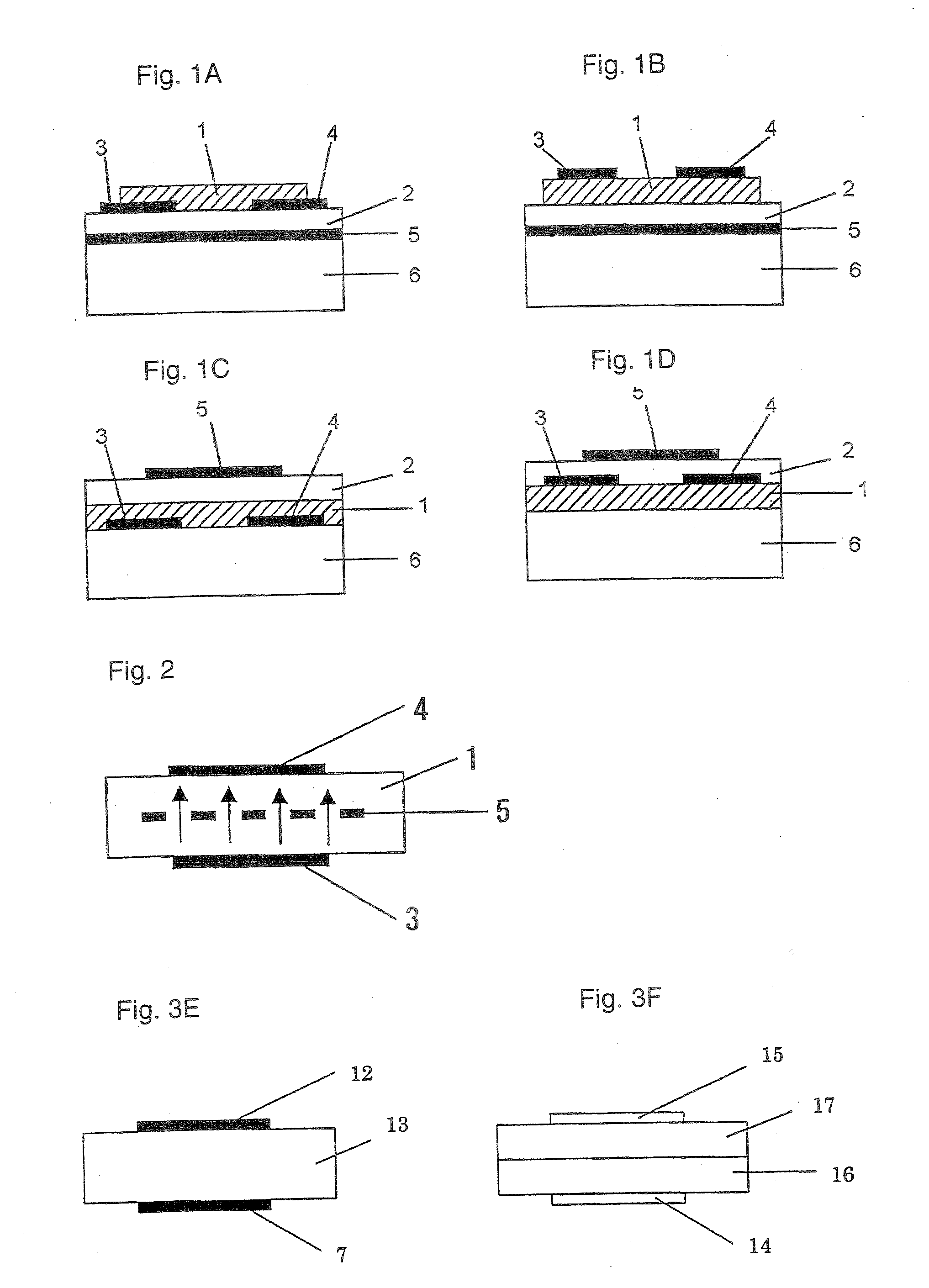
[0199] On a N-type silicon substrate (Sb-doped, resistivity: at most 0.02 Ωcm, manufactured by Sumitomo Metals Industries, Ltd.) having 300 nm of an oxide film formed thereon, gold electrodes (source and drain electrodes) having a length (L) of from 2.5 to 50 μm, a width (W) of 250 μm or a gap of 1,000 μm, were formed by photolithography. Further, the oxide film at a position different from these electrodes, was etched with a hydrofluoric acid / ammonium fluoride solution, and to the exposed Si portion, gold was vapor-deposited to form an electrode (gate electrode) to apply a voltage to the silicon substrate.
[0200] 2 mg of the bicyclo compound (1) obtained in Preparation Example 1 was dissolved in 1 ml of chloroform, and this solution was dropped between the source and drain electrodes, followed by evaporation of the solvent, and this operation was repeated a few times to obtain a good film. The X-ray diffraction of this film was observed, whereby no sharp peak was observed. Further,...
PUM
| Property | Measurement | Unit |
|---|---|---|
| temperature | aaaaa | aaaaa |
| temperature | aaaaa | aaaaa |
| ionization potential | aaaaa | aaaaa |
Abstract
Description
Claims
Application Information