Semiconductor devices

a technology of semiconductors and devices, applied in pulse generators, pulse techniques, instruments, etc., can solve the problems of inability to use another voltage and limited proposals up to the presen

Inactive Publication Date: 2007-07-05
HITACHI LTD
View PDF5 Cites 36 Cited by
  • Summary
  • Abstract
  • Description
  • Claims
  • Application Information

AI Technical Summary

Benefits of technology

[0010] It is an object of the present invention to clarify the relations therebetween, and, based on this clarification, to provide effective device structures and circuit operation conditions, or novel low-voltage circuits.
[0012] According to the present invention, it becomes possible to accomplish low-voltage implementation, low power-consumption implementation, high-speed implementation, or small-size implementation of a CMOS circuit.

Problems solved by technology

Moreover, since the circuit is operated by the single voltage VDD, it is impossible to use another voltage which would compensate for adverse influences caused by the lowering in VDD.
(2) In the conventional circuit as well, the proposals up to the present have been limited to the application to the SRAM cell.

Method used


Image

  • Semiconductor devices
  • Semiconductor devices
  • Semiconductor devices

Examples


embodiment 1

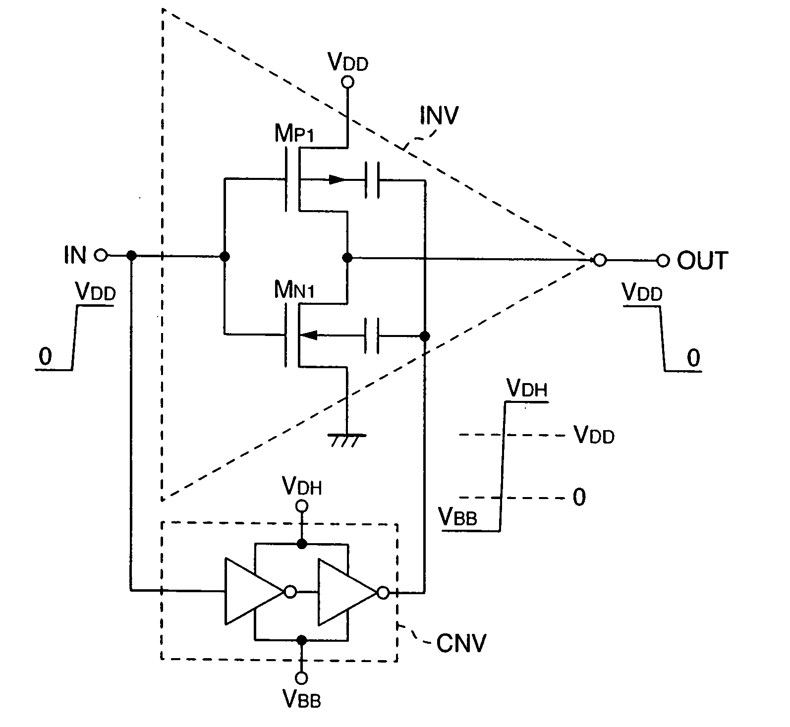
[0028]FIG. 1 illustrates a CMOS inverter circuit which is a first embodiment of the present invention. A first circuit includes, e.g., an inverter INV, and a second circuit includes, e.g., a converter CNV for controlling well voltages with large voltage amplitudes. The second circuit is a sub-circuit. This sub-circuit drives comparatively small well capacities of MOSTs within the first circuit, and thus is easy to design into small-size, high-speed, and low power-consumption implementation. In contrast thereto, the first circuit is a main-circuit. This main-circuit must generically drive large load capacities, and thus cannot help being formed into large-area, low-speed, and large power-consumption implementation. Consequently, adding the second circuit to the first one results in exertion of only a small influence on the entire area, speed, and power consumption.

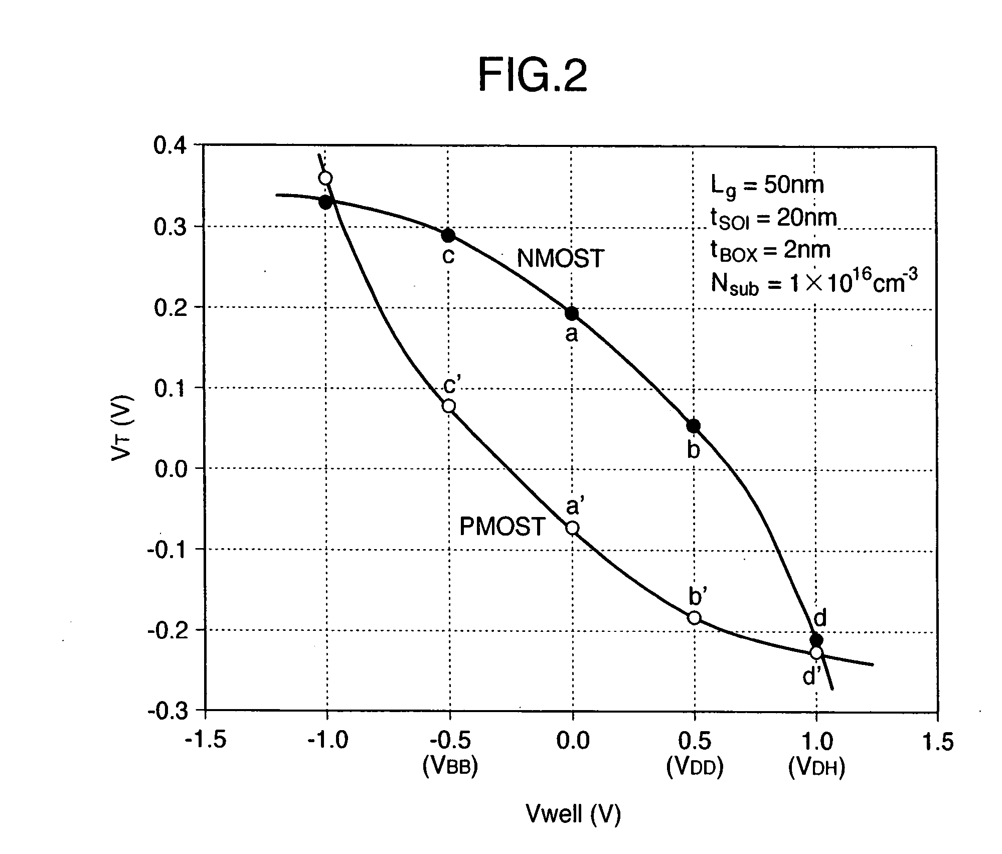
[0029] A PMOST (MP1) and an NMOST (MN1) are the FD-SOI MOST illustrated in FIG. 11 and FIG. 12. FIG. 2 illustrates the r...

embodiment 2

[0042]FIG. 4A, FIG. 4B, and FIG. 4C illustrate power-supply switches to which a MOST whose well is driven with a large voltage amplitude is applied, and which are then made small-sized. Here, a first circuit is a power-supply switch, and a second circuit is an internal core circuit (CORE). The operating voltage for the internal core circuit is small, and accordingly the threshold voltage VT of the MOST is also small. This results in flowing of a large sub-threshold current therein. FIG. 4A illustrates the following circuit: Using the PMOST (Mp), power-supply VDD for the internal core circuit is cut off from the internal core circuit during an unnecessary time-zone, thereby cutting the sub-threshold current in the internal core circuit. During the unnecessary time-zone, e.g., a time-period such as standby time or sleep mode, switching the PMOST completely OFF requires that VT of the PMOST be made larger. On the other hand, during a time-zone in which the internal core circuit operate...

embodiment 3

[0044]FIG. 5A illustrates an embodiment where the present invention is applied to a MOST switch (i.e., first circuit) and a repetition-circuit block (BLK) (i.e., second circuit). Here, this repetition-circuit block is, e.g., a word-driver block of memory. Each MOST included therein is the FD-SOI MOST. The respective sources of output PMOSTs (MW) of inverters are collectively connected to a single common source line PWL. Moreover, the PWL is connected to power-supply voltage VDD via the switch MOST (Mp). At the time of selection for an inverter, the switch MOST (Mp) is switched ON, and the input voltage into one inverter INV out of the n inverters within the block BLK is made equal to 0 V. This operation selects the one inverter INV, thus selecting and driving the corresponding one word line from among n word lines (i.e., WL0, . . . , WLn-1). On the other hand, at the time of the non-selection, the gate voltage of Mp is made equal to VDD to switch Mp OFF. Also, the input voltages int...


PUM


Abstract

A CMOS circuit in low-voltage implementation, low power-consumption implementation, high-speed implementation, or small-size implementation. In a circuit which uses a FD-SOI MOST where a back gate is controlled by a well, voltage amplitude at the well is made larger than input-voltage amplitude at the gate. Alternatively, the circuit is modified into a circuit which uses a MOST that changes dynamically into an enhancement mode and a depletion mode.

Description

CROSS-REFERENCES TO RELATED APPLICATIONS [0001] This application is a Continuation of U.S. application No. 11 / 362,172 filed on Feb. 27, 2006. Priority is claimed based on U.S. application No. 11 / 362,172 filed on Feb. 27, 2006, which claims the priority of Japanese Patent No. 2005-201054 filed Jul. 11, 2005, the entire disclosure of which is incorporated herein by reference.BACKGROUND OF THE INVENTION [0002] The present invention relates to a semiconductor device in which CMOS circuits are integrated on a semiconductor chip. More specifically, it relates to a circuit scheme and a device scheme which allow a reduction in power consumption, operating voltage, or area of a CMOS integrated circuit device. DESCRIPTION OF THE RELATED ART [0003] As is well known, in a MOS transistor (MOST), the operating voltage VDD decreases as the patterning of the MOST becomes finer. This results in an increase in the variation in threshold voltage (VT) of the MOST. For example, FIG. 10A illustrates the ...

Claims


Application Information

Patent Timeline
Patent Type & Authority Applications(United States)
IPC IPC(8): H03K3/01
CPCH01L21/84H01L27/1203H01L29/66772H03K19/018585H03K19/0027H03K19/00384H01L29/78648Y02B20/30
Inventor ITOH, KIYOOTSUCHIYA, RYUTAKAWAHARA, TAKAYUKI
Owner HITACHI LTD
Why Eureka
Try Eureka