Plated module for an IC card

a technology of ic cards and modules, applied in electrical equipment, electrical equipment, instruments, etc., can solve the problems of affecting the operation of the integrated circuit chip. , to achieve the effect of reducing the effect of these forces

Active Publication Date: 2007-07-05
STMICROELECTRONICS INT NV
View PDF10 Cites 216 Cited by
  • Summary
  • Abstract
  • Description
  • Claims
  • Application Information

AI Technical Summary

Benefits of technology

[0009] A first aim of the present invention is that of providing a plated module resistant to forces due to deforming, especially reducing the effect of these forces in proximity of the recess of a pla

Problems solved by technology

Nevertheless, since the plastic support 1 is usually kept by hand and hidden in a wallet, it is subject to damage and stress mainly with respect to the printed circuit 2 and the integrated circuit ch

Method used


Image

  • Plated module for an IC card
  • Plated module for an IC card
  • Plated module for an IC card

Examples


Embodiment Construction

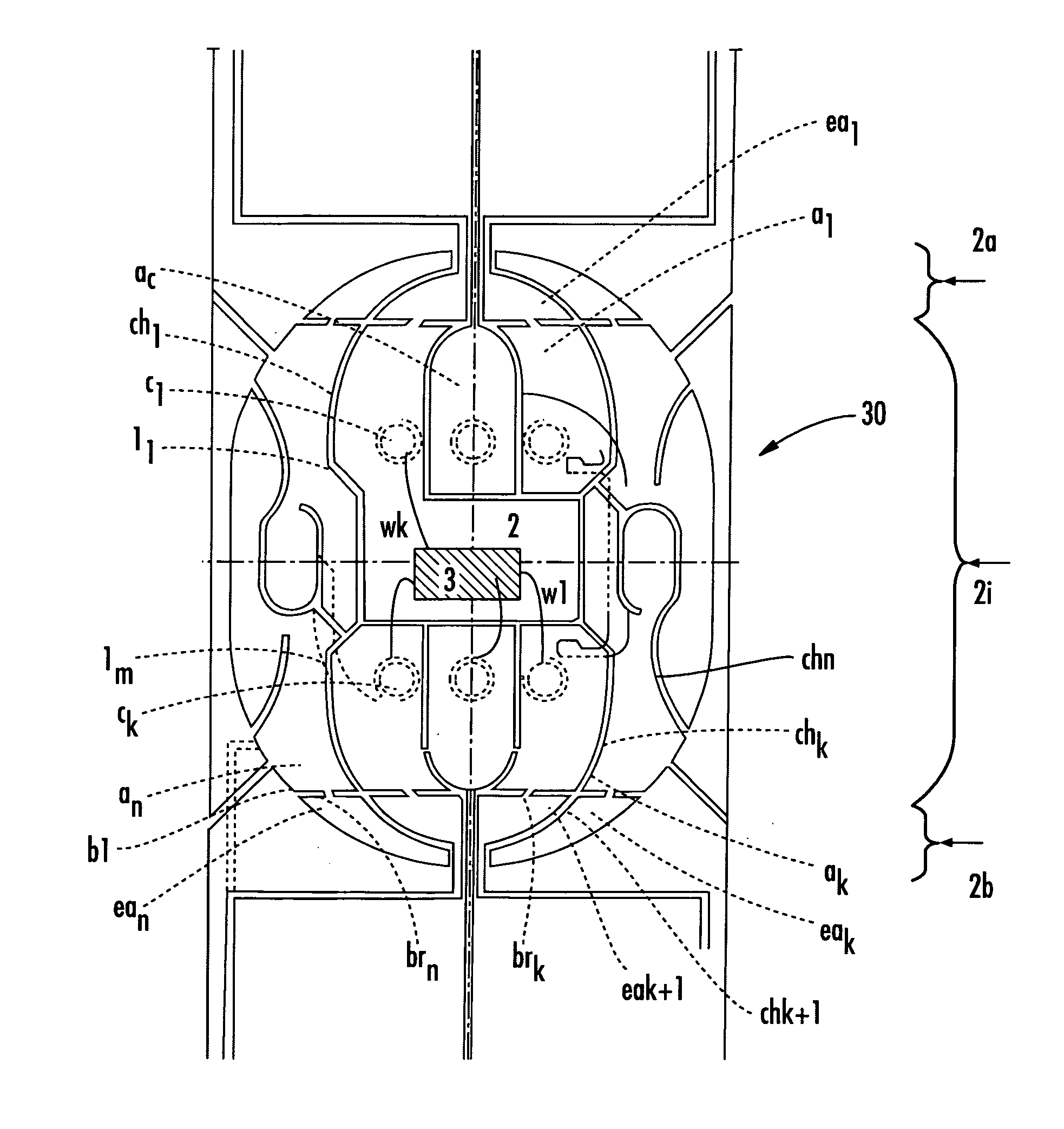
[0020] With more specific reference to FIG. 4 there is shown and is globally indicated with 30 a plated module including a printed circuit 2 comprising a plurality of conductive areas a1, . . . , an, delimited by a network of insulating channels ch1, . . . , chn, intended for covering an integrated circuit chip 3. More particularly, at least some of the conductive areas a1, . . . , an are connected through wire bonding w1, . . . , wk to a corresponding contact point c1, . . . , ck on the integrated circuit chip 3, so to provide communication connection between an external read write device 4 and the integrated circuit chip 3.

[0021] At least some of the conductive areas a1, . . . , an are linked to a corresponding extended or external area ea1, . . . , ean by one or more bridges br1, . . . , brn. A plurality of additional insulating channel ck+1 delimits an extended area eak from a nearby conductive area a1, . . . , an or from a nearby extended area ea1, . . . , eak. The insulating ...


PUM


Abstract

A plated module is for an IC card and includes a printed circuit having a plurality of conductive areas, delimited by a network of insulating channels, for covering an integrated circuit chip intended to be hosted in a recess of a plastic support of the IC card. At least some of the conductive areas are connected to a corresponding contact points of the integrated circuit chip. At least some of the conductive areas are linked to corresponding extended areas by one or more bridges. The conductive areas are separated from the extended areas by an insulating channel crossed by the bridges. The insulating channels surround the conductive areas as a protection frame for the contact points. At least a major side of at least one of the conductive areas may be curved. Several of the advanced extended areas form a rounded border of the plated module.

Description

FIELD OF THE INVENTION [0001] The present invention relates to a plated module for an IC card including a printed circuit comprising a plurality of conductive areas, delimited by a network of insulating channels, intended for covering an integrated circuit chip. BACKGROUND OF THE INVENTION [0002] As is well known, a plated or protective module is generally formed by two elements: an integrated circuit chip, and a printed circuit over the chip. With reference to FIG. 1, a plated module comprising a printed circuit 2 and an integrated circuit chip 3, is represented and globally indicated with numeral reference 20. [0003] More particularly, the printed circuit 2 comprises a plurality of conductive areas a1, . . . , an, generally glued through an epoxy resin 9. The integrated circuit chip 3 is fixed and electrically connected through wires bonding beneath the printed circuit 2, before being sealed in a recess 6 of a generic plastic support 1, as schematically represented in FIG. 2. The ...

Claims


Application Information

Patent Timeline
IPC IPC(8): H05K1/14
CPCG06K19/07728G06K19/07743G06K19/07747H01L2224/48091H01L2224/48228H01L2924/00014
Inventor FRALLICCIARDI, PAOLOVISCONTI, EDOARDO
Owner STMICROELECTRONICS INT NV
Why Eureka
Try Eureka