Method for coating semiconductor device using droplet deposition

a semiconductor device and droplet technology, applied in the field of coating of semiconductor devices, can solve the problems of increasing the overall cost and complexity, requiring costly fabrication techniques, and complex control circuits

Active Publication Date: 2007-07-12
CREELED INC
View PDF4 Cites 26 Cited by
  • Summary
  • Abstract
  • Description
  • Claims
  • Application Information

AI Technical Summary

Benefits of technology

The present invention is related to a light emitter package that includes a solid state emitter and a layer of phosphor material. The phosphor layer is deposited on the emitter through a print head nozzle, which has a small opening. The phosphor layer absorbs and down-converts some of the emitter light. The technical effect of this invention is that it provides a more efficient way to produce light emitter packages that have improved performance and efficiency.

Problems solved by technology

The technical problem addressed in this patent text is the non-uniform color temperature and difficulty in reproducing LEDs with the same or similar emission characteristics. The conventional methods for coating LEDs with a phosphor layer, such as dispensing or stencil printing, have limitations in controlling the geometry and thickness of the phosphor layer, resulting in non-uniform color temperature and LEDs that are difficult to consistently reproduce. The electrophoretic deposition method also has limitations in controlling the geometry and thickness of the phosphor layer, and can result in different concentrations of conversion material across the LEDs. The patent text proposes a new method for coating LEDs with a phosphor layer to overcome these limitations.

Method used


Image

  • Method for coating semiconductor device using droplet deposition
  • Method for coating semiconductor device using droplet deposition
  • Method for coating semiconductor device using droplet deposition

Examples


Embodiment Construction

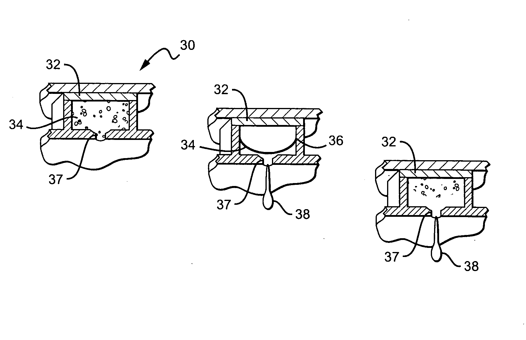
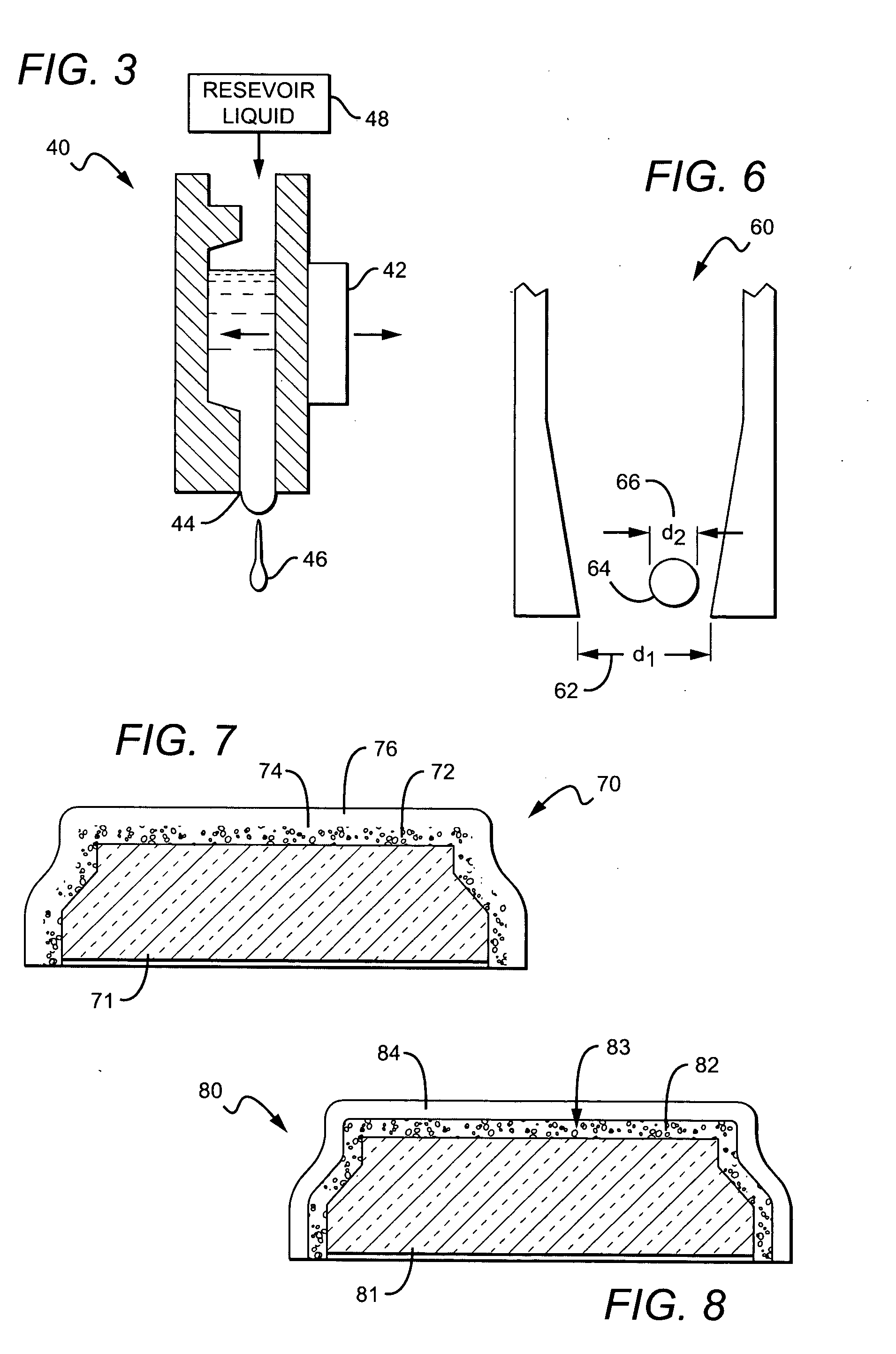
[0030] The present invention relates to a method and apparatus for conformal coating a semiconductor device with a matrix material comprised of wavelength conversion particles in a liquid medium, with the method and apparatus using jet printing technology. In particular, the wavelength conversion particles can comprise phosphor particles and the methods and apparatus can provide for conformal coating of a semiconductor device with the phosphor particles without the need for dispensing a volume of phosphor containing encapsulant, or an electric field driven deposition process.

[0031] The present invention is described herein with reference to certain embodiments but it is understood that the invention can be embodied in many different forms and should not be construed as limited to the embodiments set forth herein. The present invention is described herein with reference to a “droplet” that can be delivered to a semiconductor device, and it is understood that this term includes any c...


PUM


Abstract

Methods and systems for coating of semiconductor devices using droplets of wavelength conversion or phosphor particles in a liquid medium. A plurality of nozzles delivers a controlled amount of the matrix material to the surface of the semiconductor device, with each of said nozzles having an opening for the matrix material to pass. The opening has a diameter wherein the diameter of the phosphor particles is less than or approximately equal to one half the diameter of the opening. The phosphor particles are also substantially spherical or rounded. The nozzles are typically arranged on a print head that utilizes jet printing techniques to cover the semiconductor device with a layer of the matrix material. The methods and systems are particularly applicable to covering LEDs with a layer of phosphor materials.

Description


Claims


Application Information

Patent Timeline
Owner CREELED INC
Why Eureka
Try Eureka