Trench isolation type semiconductor device and related method of manufacture

a semiconductor device and trench isolation technology, applied in the field of trench isolation type semiconductor devices, can solve the problems of deterioration of the performance characteristics of the semiconductor device, loss (or lifting) of the insulating material filling the trench, and increase the overall manufacturing complexity, so as to minimize the junction leakage current

Active Publication Date: 2007-07-19
SAMSUNG ELECTRONICS CO LTD
View PDF15 Cites 6 Cited by
  • Summary
  • Abstract
  • Description
  • Claims
  • Application Information

AI Technical Summary

Benefits of technology

[0008]Embodiments of the invention provide a semiconductor device and manufacturing method capable of minimizing junction leakage current by preventing certain recesses in element isolation regions.

Problems solved by technology

However, the use and formation of the STI structure in not without its problems.
The inclusion of STI structures in a semiconductor device may increase the overall manufacturing complexity, and the loss (or lifting) of the insulating material filling the trench may occur, such as during a subsequently applied oxide film cleaning, or wet / dry etching process.
The presence of such leakage current causes deterioration in the performance characteristics of the semiconductor device.

Method used


Image

  • Trench isolation type semiconductor device and related method of manufacture
  • Trench isolation type semiconductor device and related method of manufacture
  • Trench isolation type semiconductor device and related method of manufacture

Examples


Embodiment Construction

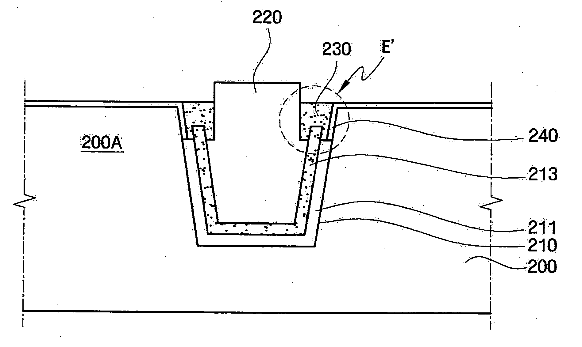
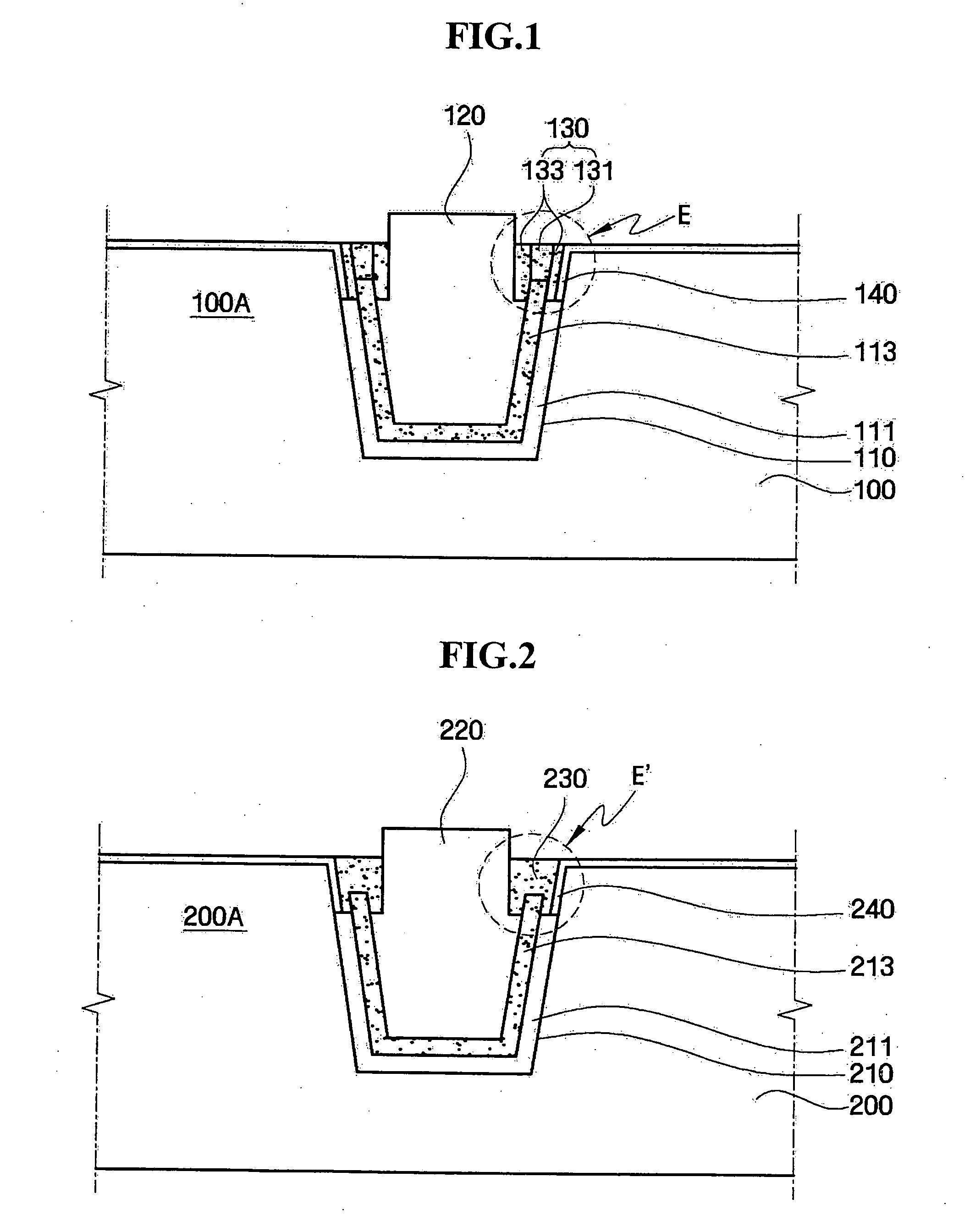
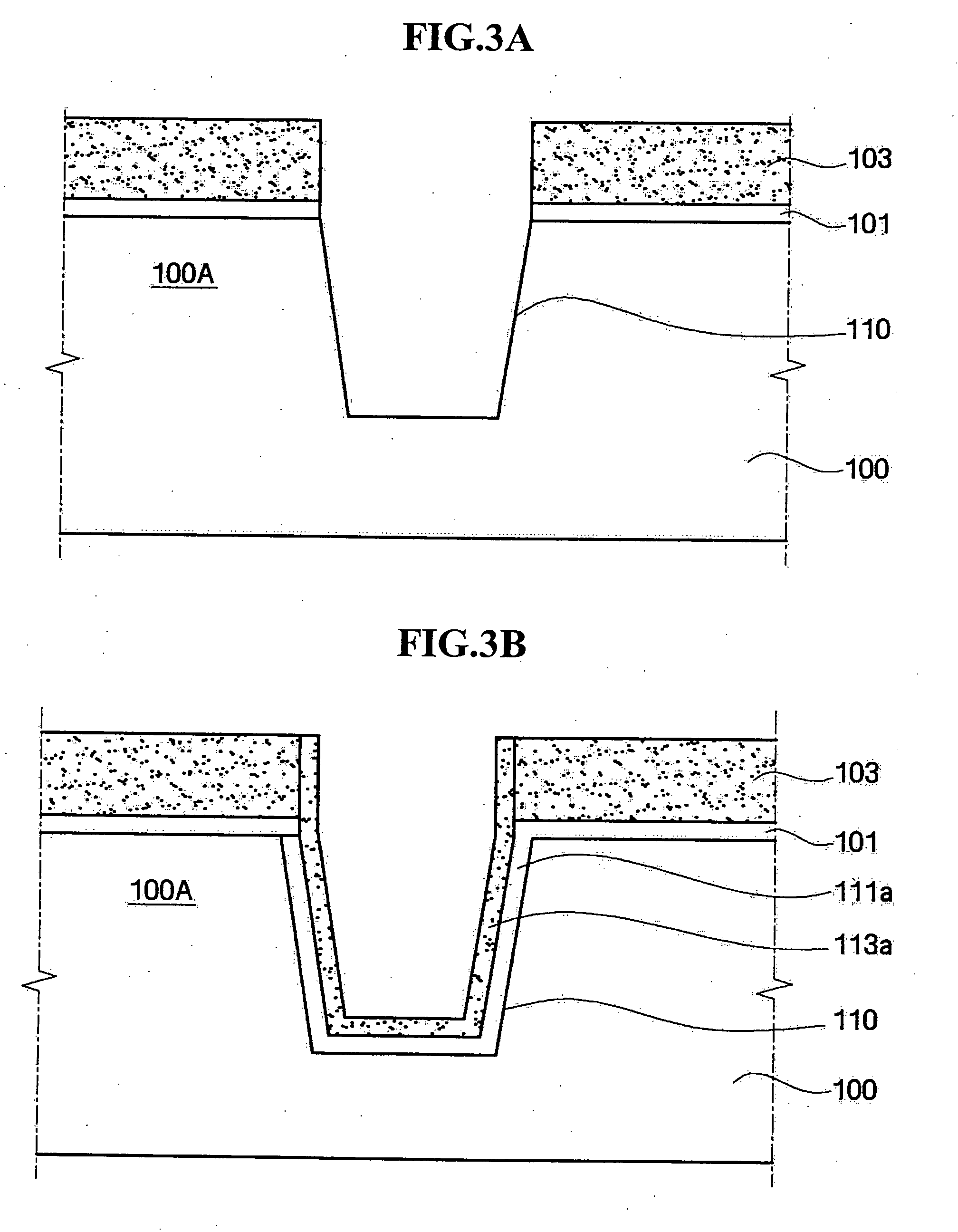
[0016]Advantages and features of the present invention and methods of accomplishing the same may be understood more readily by reference to the following description of embodiments with reference to the accompanying drawings. The present invention may, however, be embodied in many different forms and should not be construed as being limited to only the embodiments set forth herein. Rather, these embodiments are presented as teaching examples. Throughout the written description and drawings, like reference numerals refer to like or similar elements.

[0017]Embodiments of the invention will be described with reference to the cross-sectional views shown in the drawings. These views show idealized embodiments of the invention which in practical implementation may be modified or altered in their form and geometric aspect by manufacturing techniques and / or tolerances. Accordingly, the illustrated embodiments are not limited to the specific configurations shown in the drawings. For example, ...


PUM


Abstract

A semiconductor device and related method of manufacture are disclosed. The device comprises; a trench having a corner portion formed in the semiconductor substrate, a first oxide film formed on an inner wall of the trench and having an upper end portion exposing the corner portion of the semiconductor substrate, a nitride liner formed on the first oxide film, a second oxide film formed in contact with the upper end of the first oxide film and on the exposed corner portion and an upper surface of the semiconductor substrate, a field insulating film formed on the nitride liner to substantially fill the trench, and a field protecting film formed in contact with the second oxide film and filling a trench edge recess formed between the field insulating film and the second oxide film.

Description

BACKGROUND OF THE INVENTION[0001]1. Field of the Invention[0002]The present invention relates to a semiconductor device and a method of manufacturing the same. More particularly, the invention relates to a trench isolation type semiconductor device having reduced junction leakage current in an element isolation region, and a related method of manufacture.[0003]This application claims priority from Korean Patent Application No. 10-2006-0004115 filed on Jan. 13, 2006, the subject matter of which is hereby incorporated by reference in its entirety.[0004]2. Description of the Related Art[0005]A semiconductor device commonly includes a plurality of active and passive elements formed on a semiconductor substrate. Different types of semiconductor devices perform different functions depending on how the various elements are arranged and electrically connected. Accordingly, most of the elements forming a particular semiconductor device must be electrically isolated from one or more adjacent ...

Claims


Application Information

Patent Timeline
Patent Type & Authority Applications(United States)
IPC IPC(8): H01L29/00
CPCH01L21/76224H01L21/76
Inventor YOUN, KI-SEOGAHN, JONG-HYONROH, KWAN-JONGLEE, HYE-KYOUNG
Owner SAMSUNG ELECTRONICS CO LTD
Why Eureka
Try Eureka