

Multilayer piezoelectric devices and method of producing same
- Summary
- Abstract
- Description
- Claims
- Application Information
AI Technical Summary
Benefits of technology
Problems solved by technology
Method used
Image

Examples
example 1
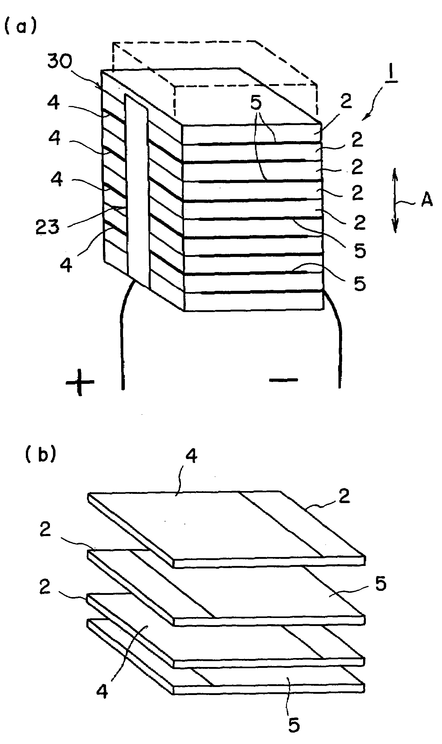
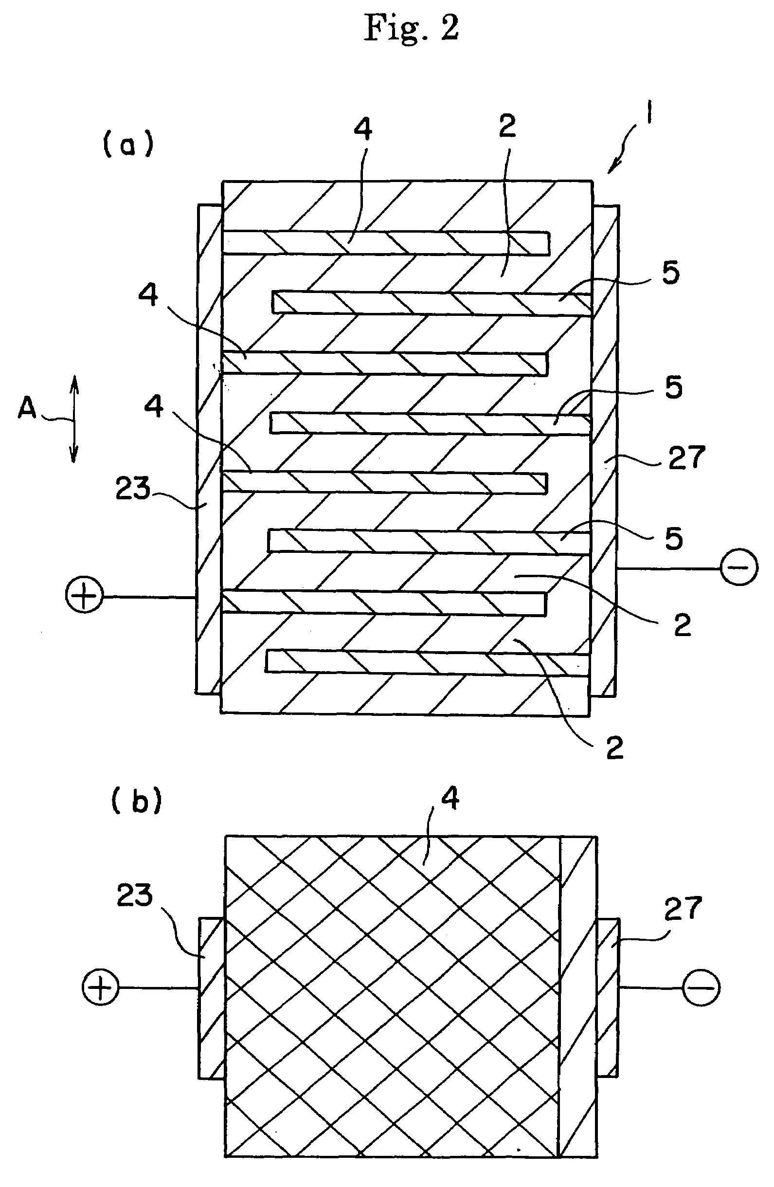
[0087]A device shown in FIGS. 1-3 was constructed. Specifically, 300-350 layers for constituting an active region and 50 layers each for constituting the upper or lower inactive regions were integrated by lamination. An internal electrode layer (e.g. 3 μm in thickness) was printed on each section of a piezoelectric tape and an adhesive layer (e.g. 5 μm in thickness) with an increased binder content as compared with the tape was printed thereon, and the layers were integrated by heating at 80° C. and weighting at 2 MPa.
[0088]The thus-integrated laminated molding was degreased at 600° C. and fired at 900-1100° C. to give a laminated piezoelectric ceramics body. This laminated body was cut and ground smooth to give a laminated body having a desired shape. The cross-section of the laminated body was 7 mm×7 mm in size and the length thereof was 35 mm. A underlying layer 3 to serve as an external electrode was formed on each of two sides of the device with offset electrode layers drawn ou...
PUM
 Abstract
Description
Claims
Application Information