
Output circuit

Inactive Publication Date: 2007-08-02
FUJITSU LTD
View PDF1 Cites 12 Cited by
  • Summary
  • Abstract
  • Description
  • Claims
  • Application Information

AI Technical Summary

Benefits of technology

[0007] An object of the present invention is to prevent malfunction caused by the power noise by reducing the power noise in the tri-state output circuit.
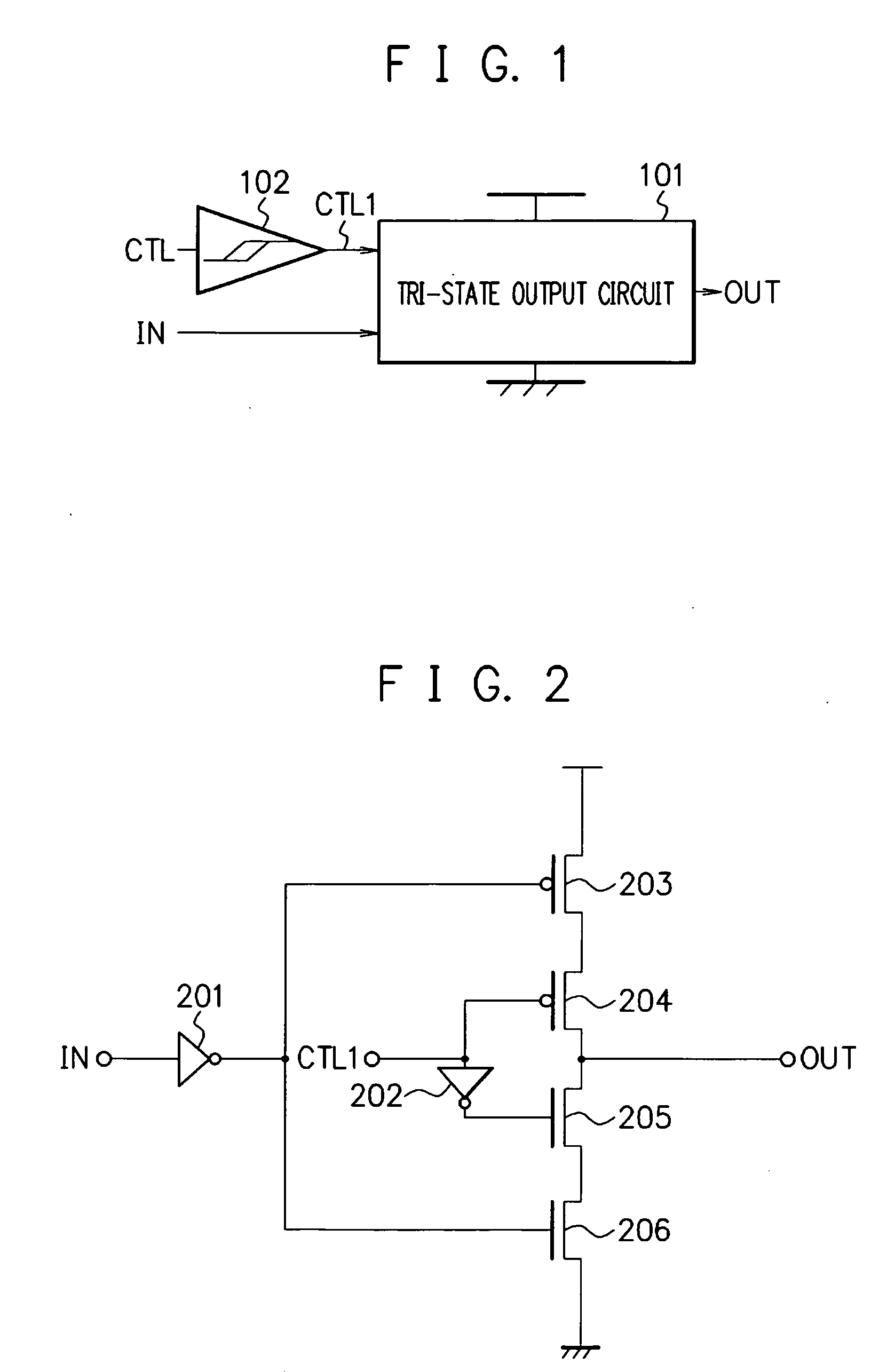
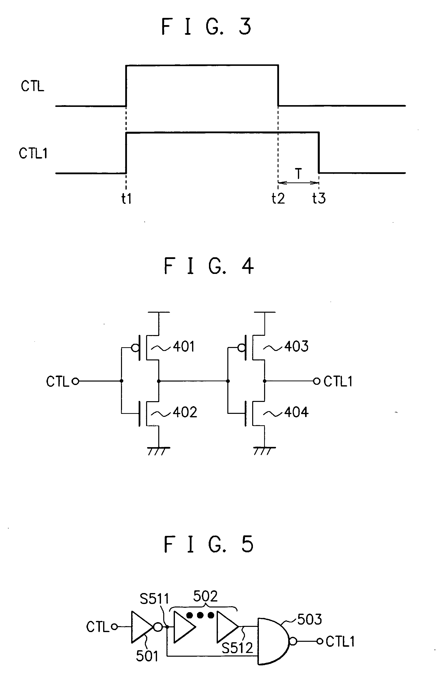
[0008] According to an aspect of the present invention, an output circuit including: a tri-state output circuit capable of outputting high-impedance state, high-level state, and low-level state, in which the high-level state and low-level state are low-impedance state, and switching the high-impedance state and the low-impedance state in accordance with a first control signal; and a delay circuit outputting the first control signal to the tri-state output circuit by inputting a second control signal and delaying the second control signal so that timing delay time of the second control signal switching the high-impedance state to the low-impedance state is longer than the timing delay time of the second control signal switching the low-impedance state to the high-impedance state, is provided.

Problems solved by technology

Along with increasing power noise backed by current consumption increase in an LSI and lowering voltage in an internal circuit of the LSI, the need to reduce the power noise is increasing.
In addition to the noise arising from the simultaneous switching of the plurality of I / O cells, power noise sometimes arises in a single tri-state output circuit.

Method used


Image

  • Output circuit
  • Output circuit
  • Output circuit

Examples


Embodiment Construction

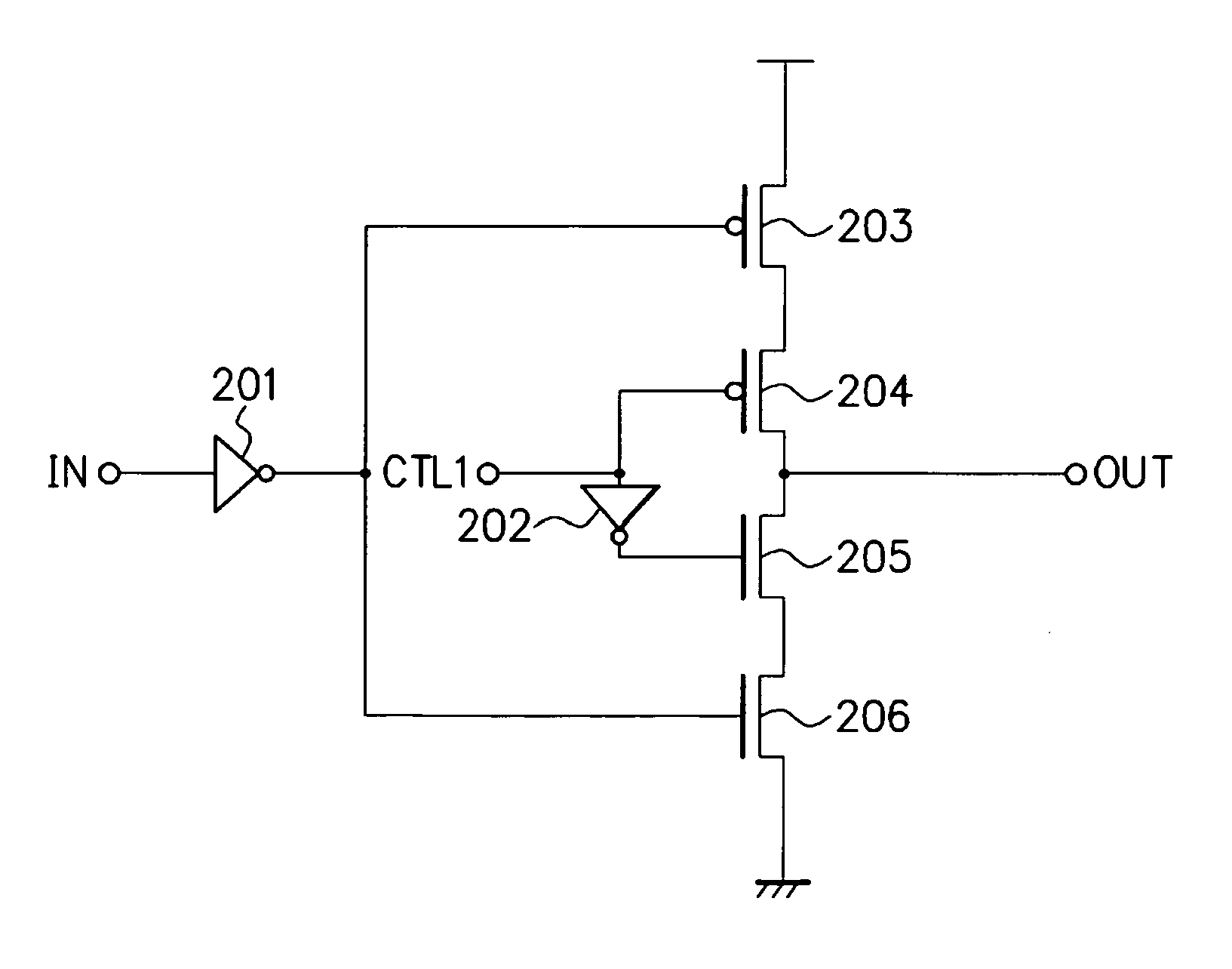
[0027]FIG. 15 is a view showing a tri-state output circuit 101 and FIG. 16 is a timing chart to explain its operation. Note that an input signal IN and a control signal CTL are shown in FIGS. 16 and 17 by slightly shifting their voltages for the purpose of distinguishing their level transitions. In actual, the input signal IN and the control signal CTL are at 0 (zero) V in their low level and at 1.3 V in their high level. A power supply voltage VDD is 3.3 V and a reference voltage VSS is 0 (zero) V.

[0028] The tri-state output circuit 101 is connected to between the power supply voltage VDD and the reference voltage VSS, and inputs the control signal CTL and the input signal IN and outputs an output signal OUT. When the control signal CTL is at low level and the input signal IN is at high level, the output signal OUT is also in a high-level state, and when the control signal CTL is at low level and the input signal IN is at low level, the output signal OUT is also in a low-level sta...


PUM


Abstract

An output circuit including: a tri-state output circuit capable of outputting high-impedance state, high-level state, and low-level state, in which the high-level state and low-level state are low-impedance state, and switching the high-impedance state and the low-impedance state in accordance with a first control signal; and a delay circuit outputting the first control signal to the tri-state output circuit by inputting a second control signal and delaying the second control signal so that timing delay time of the second control signal switching the high-impedance state to the low-impedance state is longer than the timing delay time of the second control signal switching the low-impedance state to the high-impedance state, is provided.

Description

CROSS-REFERENCE TO RELATED APPLICATIONS [0001] This application is based upon and claims the benefit of priority from the prior Japanese Patent Application No. 2006-023249, filed on Jan. 31, 2006, the entire contents of which are incorporated herein by reference. BACKGROUND OF THE INVENTION [0002] 1. Field of the Invention [0003] The present invention relates to an output circuit. [0004] 2. Description of the Related Art [0005] Along with increasing power noise backed by current consumption increase in an LSI and lowering voltage in an internal circuit of the LSI, the need to reduce the power noise is increasing. Of these noises, for the noise arising from simultaneous switching of an I / O cell, a method with which noise arising from simultaneous switching of a plurality of I / O cells can be reduced is proposed (Patent document 1: Japanese Patent Application Laid-Open No. 2004-334271). [0006] In addition to the noise arising from the simultaneous switching of the plurality of I / O cell...

Claims


Application Information

Patent Timeline
IPC IPC(8): H03K19/00
CPCH03K19/09429H03K19/00361
Inventor KAWABE, YUKIHITO
Owner FUJITSU LTD
Learn More