
Method for transmitting a burst in optical burst switching system

a switching system and optical burst technology, applied in data switching networks, frequency-division multiplexes, instruments, etc., can solve the problems of degrading channel utilization and system performance, and the empty void between survived data bursts is not well utilized, so as to maximize system performance and improve channel utilization

Inactive Publication Date: 2007-08-02
KOREA ADVANCED INST OF SCI & TECH
View PDF3 Cites 7 Cited by
  • Summary
  • Abstract
  • Description
  • Claims
  • Application Information

AI Technical Summary

Benefits of technology

[0010] It is an object of the present invention to provide a method for transmitting a burst in an optical burst switching system, which is capable of improving channel utilization and maximizing system performance by inserting and transmitting a data burst which originates from a current node and whose destination is a next node, into an empty void between data bursts that survive competition to occupy an output channel among data bursts transmitted to the next node by way of the current node.

Problems solved by technology

In conventional art, however, such an empty void between survived data bursts is not well utilized.
This degrades channel utilization and system performance.

Method used


Image

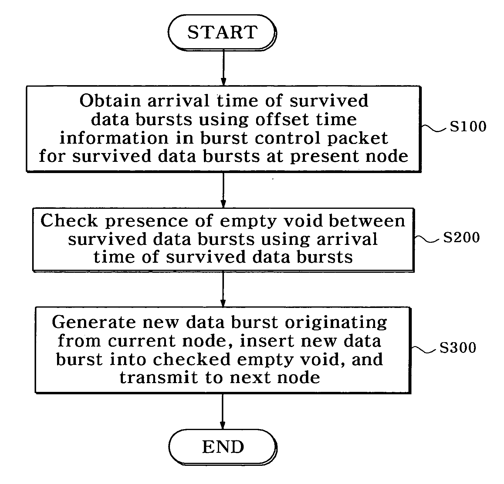
  • Method for transmitting a burst in optical burst switching system
  • Method for transmitting a burst in optical burst switching system
  • Method for transmitting a burst in optical burst switching system

Examples


Embodiment Construction

[0020] The present invention will now be described more fully with reference to the accompanying drawings, in which exemplary embodiments of the invention are shown.

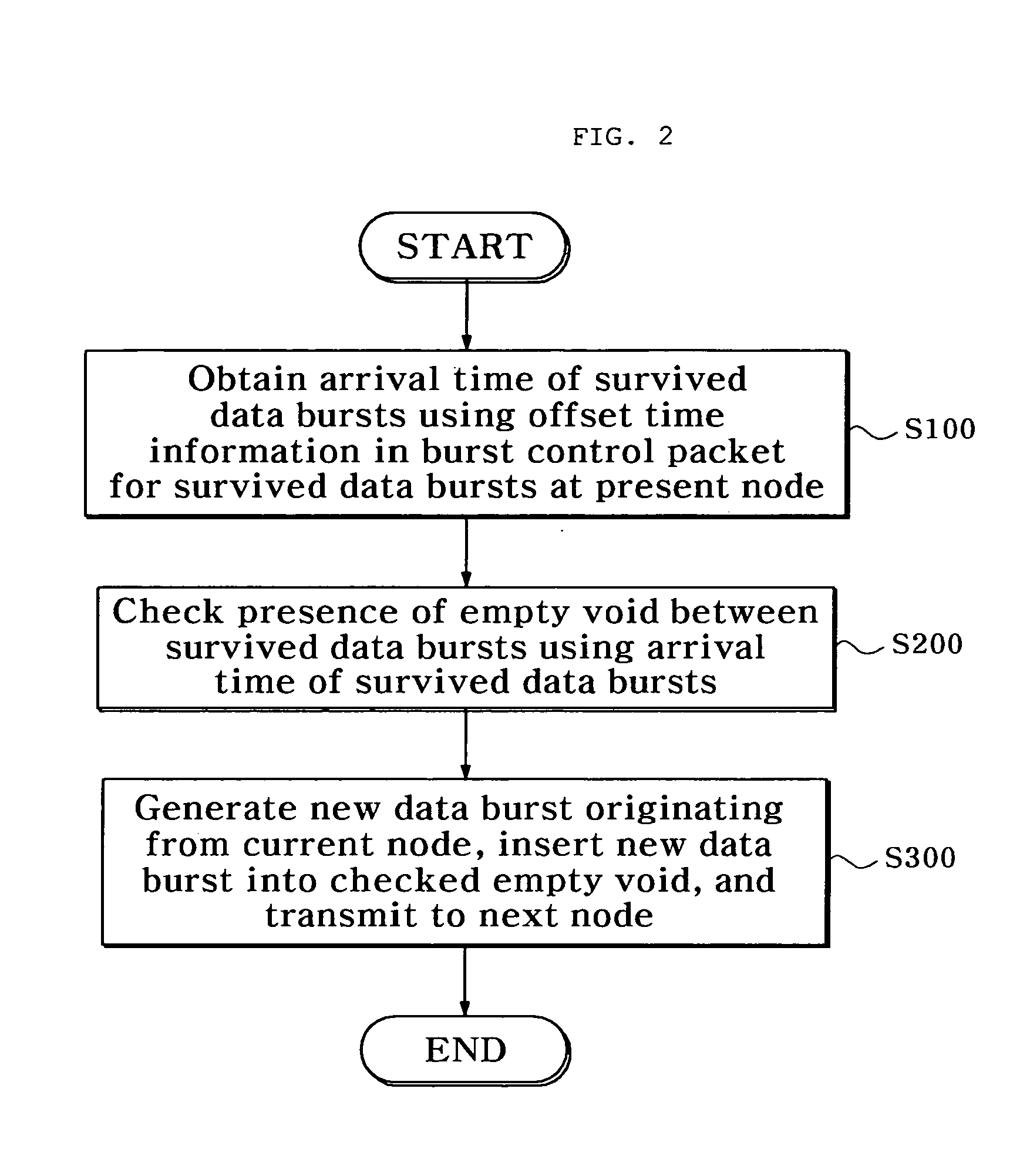
[0021]FIG. 2 is a flowchart illustrating a method for transmitting a burst in an optical burst switching system according to an exemplary embodiment of the present invention.

[0022] Referring to FIG. 2, an arrival time of data bursts that survive competition to occupy an output channel among data bursts transmitted to a next node by way of a current node is obtained using offset time information in burst control packets for the survived data bursts (S100).

[0023] The presence of an empty void between the survived data bursts is then checked using the obtained arrival time of the survived data bursts (S200).

[0024] A new data burst originating from the current node is then generated. The new data burst is inserted into the checked empty void and transmitted to the next node (S300).

[0025] At this time, if a burst control...


PUM


Abstract

Provided is a method for transmitting a burst in an optical burst switching system, in which when a burst is generated at an originating node, a burst control packet is transmitted to a destination node by way of a plurality of nodes and then a data burst is transmitted after a pre-allocated offset time. The method includes the steps of obtaining an arrival time of data bursts that survive competition to occupy an output channel among data bursts transmitted to the next node by way of the current node using offset time information in burst control packets for the survived data bursts, checking whether an empty void is present between the survived data bursts by using the obtained arrival time of the survived data bursts, and generating a new data burst originating from the current node, inserting the newly generated data burst into the checked empty void, and transmitting to the next node. This method can improve channel utilization and maximize performance of the optical burst switching system.

Description

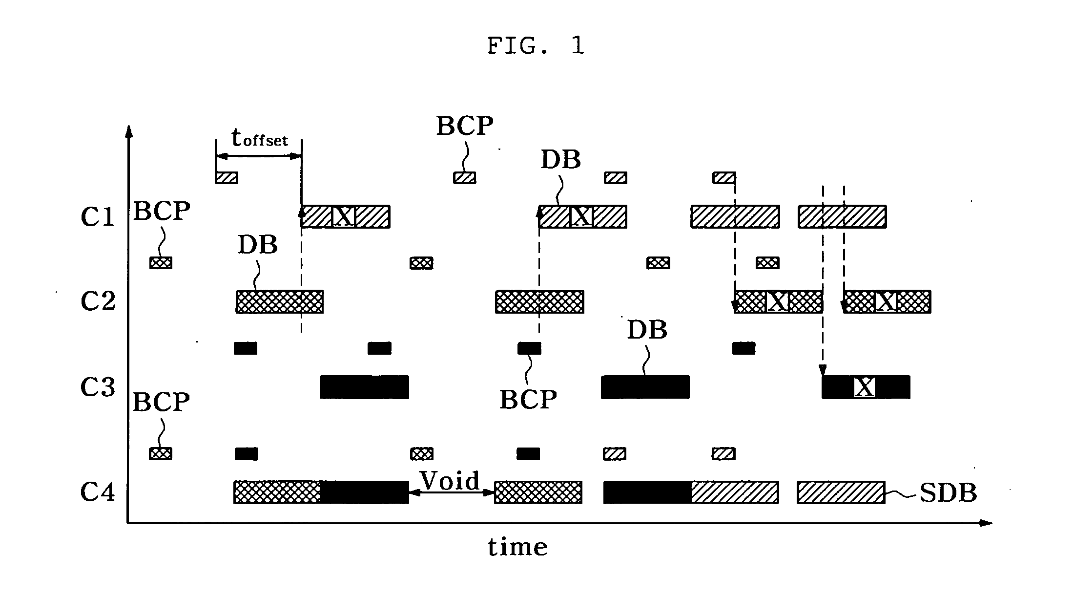
BACKGROUND OF THE INVENTION [0001] 1. Field of the Invention [0002] The present invention relates to a method for transmitting a burst in an optical burst switching system, and more particularly, to a method for transmitting a burst in an optical burst switching system that is capable of improving channel utilization and thus maximizing system performance by inserting and transmitting a data burst which originates from a current node and whose destination is a next node, into an empty void between data bursts that survive competition to occupy an output channel among data bursts transmitted to the next node by way of the current node. [0003] 2. Description of the Related Art [0004] In a conventional optical burst switching system, a burst control packet (BCP) is first transmitted when a burst is generated. After a certain time elapses, a data burst (DB), which is a burst for transmitting real data, is transmitted. This time difference is called an offset time. [0005] Such method for...

Claims


Application Information

Patent Timeline
Patent Type & Authority Applications(United States)
IPC IPC(8): H04L12/56H04L12/801H04L12/911H04L12/931H04L12/937
CPCH04Q2011/0064H04Q11/0066H04B10/25H04Q11/00
Inventor LEE, SEOUNG YOUNGHWANG, IN YONGPARK, HONG SHIK
Owner KOREA ADVANCED INST OF SCI & TECH
Learn More