Method for forming a stud bump

Inactive Publication Date: 2007-08-16
SHINKAWA CO LTD
View PDF3 Cites 22 Cited by
  • Summary
  • Abstract
  • Description
  • Claims
  • Application Information

AI Technical Summary

Benefits of technology

[0018]The object of the present invention is to provide a method for forming a stud bump wherein it is unnecessary to add any special equipment for executing wire cutting, and wherein stud bumps can be formed while freely controlling the height.
[0027]As seen from the above, a scratch is made by a capillary in the portion of a wire located above the bonded ball, and this scratched portion is bent to make it easy to cut, and, after that, a stud bump is formed by the actions of the ascending motion of the capillary and of the closing motion of the clamper. Accordingly, there is no necessity to add any special wire cutting equipment to the wire bonding apparatus or bump bonding apparatus. Also, the height of the stud can be controlled by the height to which the capillary is made to ascend after bonded ball formation. Accordingly, stud height can be set freely or any desired height for a stud is obtainable.

Problems solved by technology

In such cases, in a multiple-pin die in which a large number of stud bumps are provided, the gap between the pins are narrow, stud bump resistance is large, and it is difficult for the adhesives to reach all the way between the gaps.

Method used


Image

  • Method for forming a stud bump
  • Method for forming a stud bump

Examples


Embodiment Construction

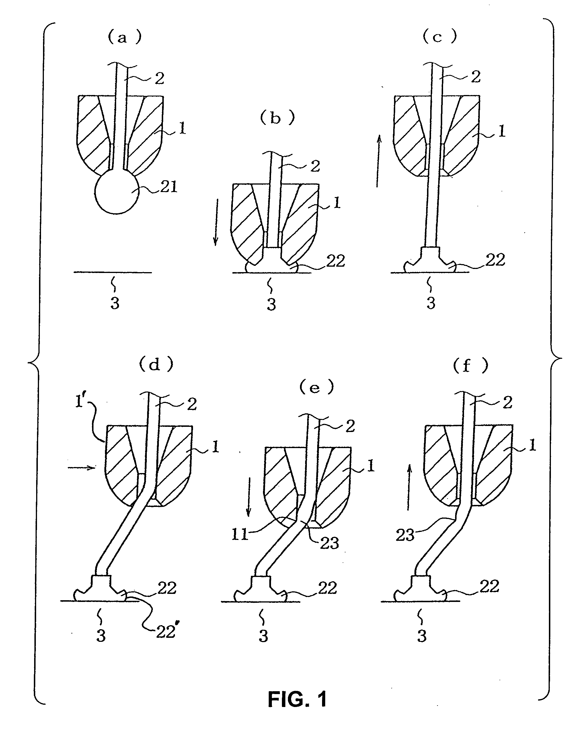
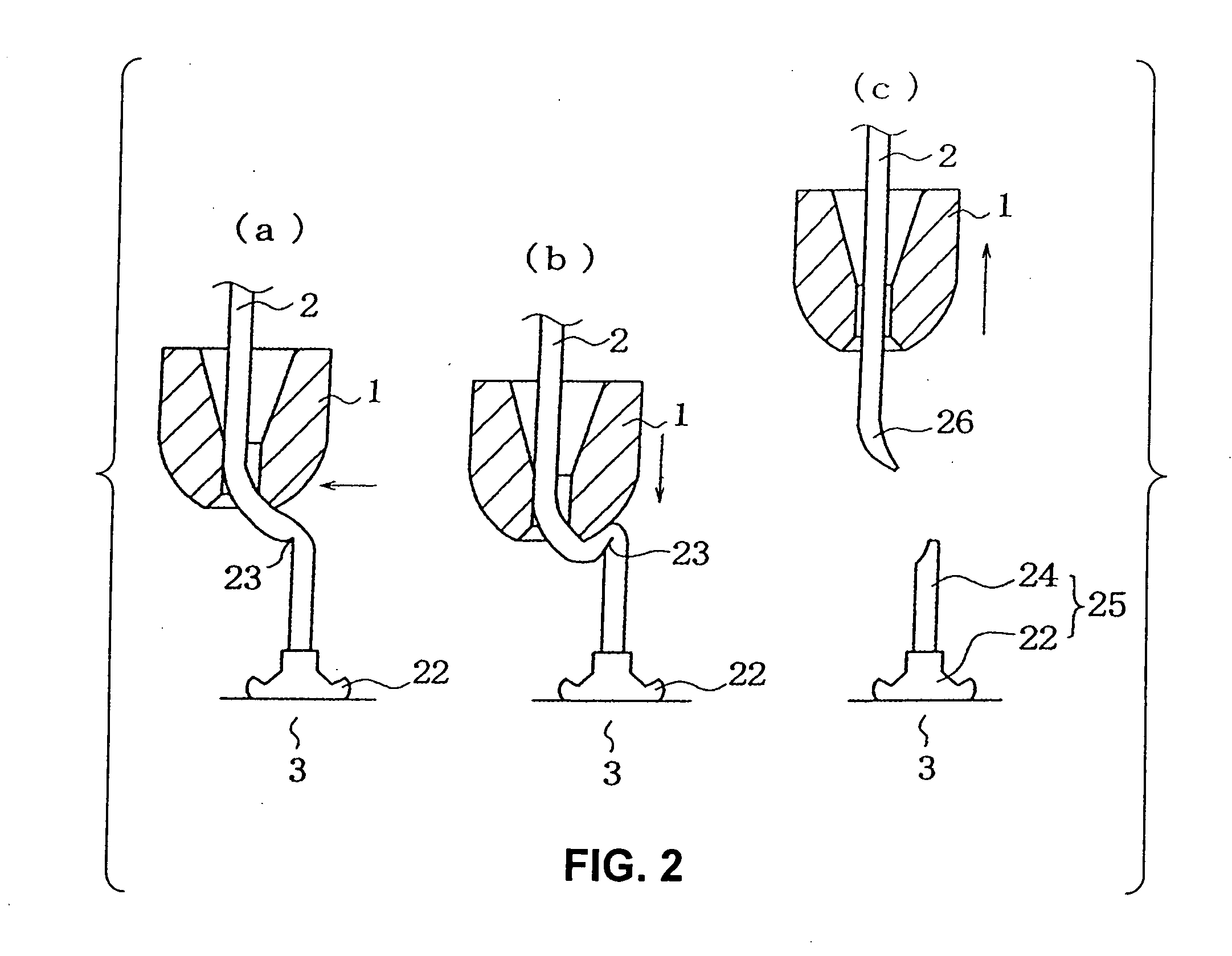
[0030]One embodiment of the method for forming a stud bump of the present invention will be described below with reference to FIG. 1 and FIG. 2, which is continued from FIG. 1.

[0031]In step (a) shown in FIG. 1, at the tip end of a wire 2 passing through a damper (not shown) and a capillary 1, a ball 21 is formed by an electric flame off probe (not shown), and then the clamper is opened.

[0032]Next, in step (b) of FIG. 1, the capillary 1 is caused to descend toward the pad 3, and the ball 21 is bonded to a pad 3 to form a bonded ball 22 on the pad 3.

[0033]In next step (c), the capillary 1 is caused to ascend for an arbitrary distance above the pad 3 to an arbitrary height.

[0034]Following that, in step (d), the capillary 1 is moved in a lateral direction or substantially parallel to the surface of the pad 3. More specifically, the capillary 1 is moved laterally (to the right-hand side in the shown embodiment of FIG. 1) for a distance that the outer surface (left-hand side surface 1′) o...


PUM


Abstract

A method for forming stub bumps in, for instance, semiconductor device fabrication, including a bonded ball formation step for bonding a ball formed at a tip end of a wire passing through a capillary to a pad to form a bonded ball on the pad; a scratching step for, next, scratching a portion of the wire above the bonded ball with an interior edge of the capillary by moving the capillary; a bending step for, next, bending the scratched portion of the wire by moving the capillary; and a cutting step for, thereafter, cutting the wire from the scratched portion by closing a damper during an ascending motion of the capillary.

Description

BACKGROUND OF THE INVENTION[0001]The present invention relates to a method for forming a stud bump in, for instance, semiconductor device fabrication.[0002]A stud bump is a bonded ball, which is bonded to a die pad and has a wire (stud or standing wire) of a predetermined length (height). Such a stud bump is formed by a wire bonding apparatus or a bump bonding apparatus. The stud bumps formed on a die and conductors formed on a circuit board are bonded by a flip-chip bonding method.[0003]In a semiconductor device that includes the above-described connections, in order to bond strongly a die and a circuit board, an adhesive is put between the two. In such cases, in a multiple-pin die in which a large number of stud bumps are provided, the gap between the pins are narrow, stud bump resistance is large, and it is difficult for the adhesives to reach all the way between the gaps. This circumstance has led, recently, to a demand for stud bumps having greater stud heights.[0004]Japanese P...

Claims


Application Information

Patent Timeline
IPC IPC(8): A47J36/02
CPCH01L24/11H01L2224/1134H01L2224/13099H01L2924/01082H01L2924/01006H01L2924/01033H01L2924/00013H01L2924/01005H01L2924/00014H01L24/13H01L24/742H01L2224/742
Inventor TOYAMA, TOSHIHIKOMII, TATSUNARI
Owner SHINKAWA CO LTD
Why Eureka
Try Eureka