Semiconductor Device with both I/O and Core Components and Method of Fabricating Same

Inactive Publication Date: 2008-12-25
TAIWAN SEMICON MFG CO LTD
View PDF8 Cites 6 Cited by
  • Summary
  • Abstract
  • Description
  • Claims
  • Application Information

AI Technical Summary

Benefits of technology

[0018]Advantages of the present invention include an I / O device that retains desirable properties without the need to alter the high-k process used in forming the core device; the I / O device may be formed without a high-k dielectric layer while the core device may use a high-k dielectric with either a poly or a metal gate. In preferred embodiments of the present invention, an addition mask for I / O device integration is unnecessary and ion implantation through oxide for the I / O device may be avoided.

Problems solved by technology

As the size of these popular devices would imply, the components formed on a chip are extremely small.
There are differences, however, that affect the fabrication of such devices on the same wafer.
The I / O device, on the other hand, may have to handle a higher voltage, however, so it cannot always be fabricated to the specifications best suited for the core device.

Method used


Image

  • Semiconductor Device with both I/O and Core Components and Method of Fabricating Same
  • Semiconductor Device with both I/O and Core Components and Method of Fabricating Same
  • Semiconductor Device with both I/O and Core Components and Method of Fabricating Same

Examples


Embodiment Construction

[0026]The making and using of the presently preferred embodiments are discussed in detail below. It should be appreciated, however, that the present invention provides many applicable inventive concepts that can be embodied in a wide variety of specific contexts. The specific embodiments discussed are merely illustrative of specific ways to make and use the invention, and do not limit the scope of the invention.

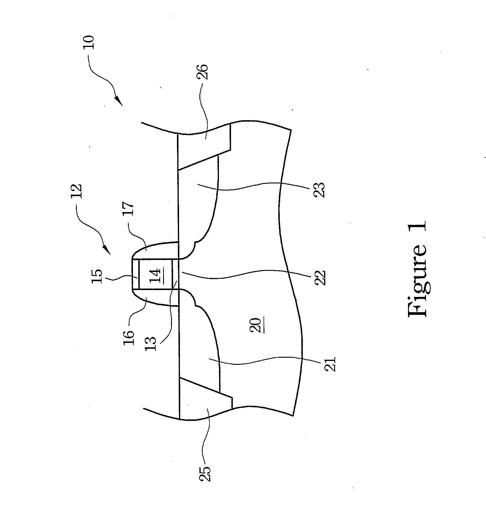
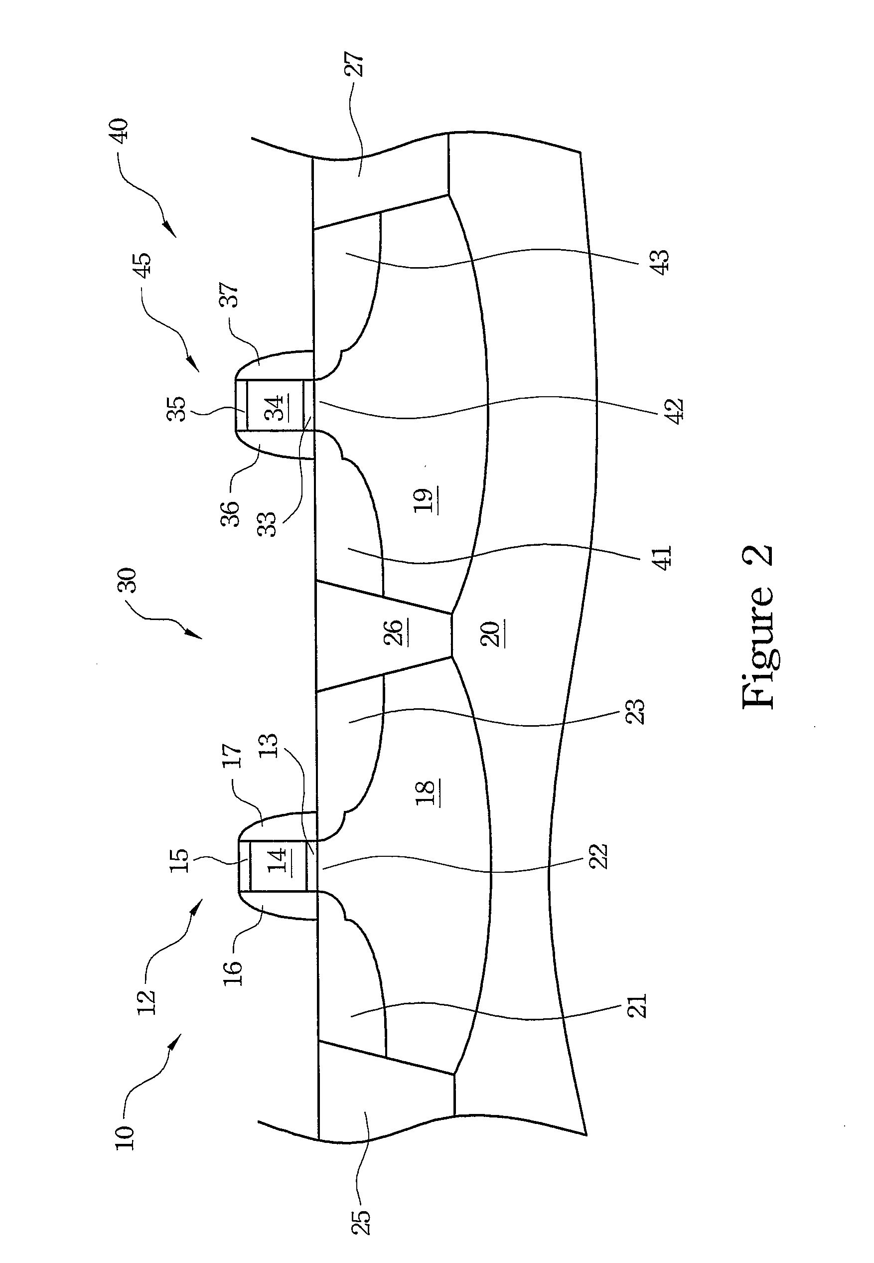
[0027]The present invention will be described with respect to preferred embodiments in a specific context, namely a semiconductor device having a resistor, and having a core device and an I / O device that are both MOS (metal oxide semiconductor) transistors. The invention may also be applied, however, to other semiconductor devices as well.

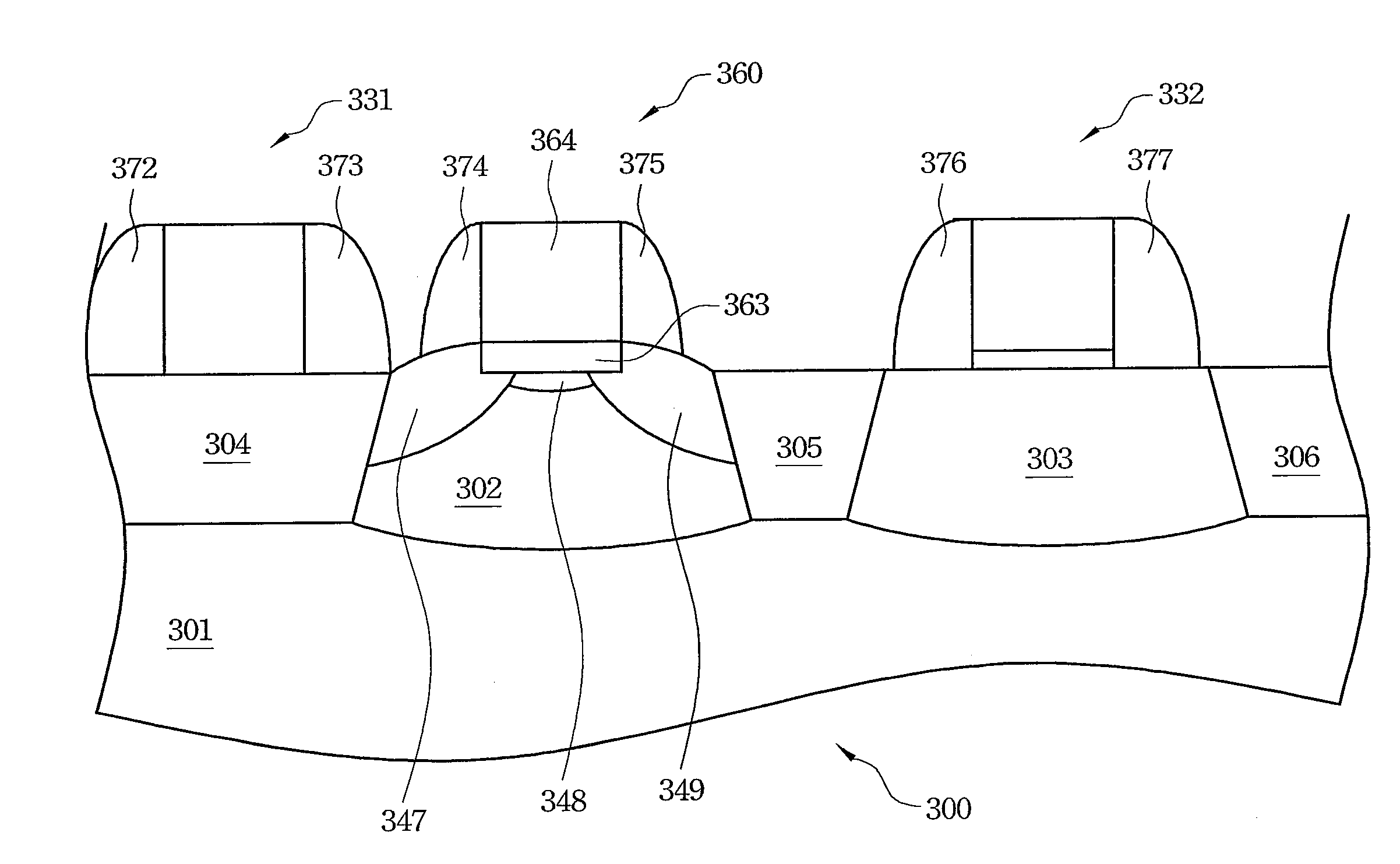
[0028]FIG. 3 is a side view illustrating in cross-section a semiconductor device 100 according to an embodiment of the present invention. Semiconductor device 100 includes a substrate 101 having a core well 102 and an I / O well 103 separated ...


PUM


Abstract

A semiconductor device having a core device with a high-k gate dielectric and an I / O device with a silicon dioxide or other non-high-k gate dielectric, and a method of fabricating such a device. A core well and an I / O well are created in a semiconductor substrate and separated by an isolation structure. An I / O device is formed over the I / O well and has a silicon dioxide or a low-k gate dielectric. A resistor may be formed on an isolation structure adjacent to the core well. A core-well device such as a transistor is formed over the core well, and has a high-k gate dielectric. In some embodiments, a p-type I / O well and an n-type I / O well are created. In a preferred embodiment, the I / O device or devices are formed prior to forming the core device and protected with a sacrificial layer until the core device is fabricated.

Description

TECHNICAL FIELD[0001]The present invention relates generally to the field of fabricating semiconductor devices, and relates more particularly to the fabrication of a reliable semiconductor device that included an I / O (input / output) device and a core device, and a method for fabricating such a device.BACKGROUND[0002]Generally, semiconductor devices are very small electronic components that are fabricated on a semiconductor wafer substrate. Using a variety of fabrication techniques, these devices are made and connected together to form integrated circuits. A number of integrated circuits may be found on one chip, and are capable of performing a set of useful functions in the operation of an electronic appliance. Examples of such electronic appliances are mobile telephones, personal computers, and personal gaming devices. As the size of these popular devices would imply, the components formed on a chip are extremely small.[0003]There are many kinds of semiconductor components. Transist...

Claims


Application Information

Patent Timeline
IPC IPC(8): H01L29/76H01L27/12H01L27/01H01L31/0392
CPCH01L21/823412H01L21/823418H01L21/823462H01L27/0629H01L27/088H01L27/0922H01L29/7848H01L29/66477
Inventor CHENG, CHUNG LONGCHUNG, SHENG-CHENTHEI, KONG-BENGCHUANG, HARRYLIANG, MONG SONG
Owner TAIWAN SEMICON MFG CO LTD
Why Eureka
Try Eureka