Method for fabricating semiconductor device

a semiconductor and device technology, applied in the direction of semiconductor devices, basic electric elements, electrical equipment, etc., can solve the problems of inapplicability to the combined fabrication process of flash memory cells, method is not compatible with borderless contact, and damage to the contact part of the substrate, so as to prevent the change of characteristics of peripheral transistors, increase the fabrication cost, and complicate the fabrication process

Active Publication Date: 2009-07-07
FUJITSU SEMICON LTD
View PDF10 Cites 10 Cited by
  • Summary
  • Abstract
  • Description
  • Claims
  • Application Information

AI Technical Summary

Benefits of technology

[0016]An object of the present invention is to provide a method for fabricating a semiconductor device which facilitates the fabricating a logic semiconductor device combined with a nonvolatile semiconductor memory without making the fabricating process complicated and ensuring the compatibility with the fabrication process of the leading logic device.
[0019]According to the present invention, in the method for fabricating a logic semiconductor device combined with a nonvolatile memory transistor of the stack gate structure, in the multiple oxidation process for forming plural kinds of gate insulating films of different film thicknesses, the inter-gate insulating film in the region for the contact to the gate electrode of the conductive layer of the same level as the floating gate is removed, whereby the semiconductor substrate and the device isolation film are prevented from being damaged by the etching for removing the inter-gate insulating film. Thus, changes of the characteristics of the peripheral transistors can be prevented.
[0020]The inter-gate insulating film in the region for the contact to the gate electrode of the conductive layer of the same level as the floating gate can be only by adding to the mask pattern to be used in the multiple oxidation process the opening exposing the region for the contact to be formed, which makes it unnecessary to add a photoresist step, which much increases the fabrication cost.
[0021]Before the inter-layer insulating film is formed, the inter-gate insulating film in the region for the contact to the gate electrode of the conductive layer of the same level as the floating gate is removed in advance before the inter-layer insulating film is formed, which makes it possible to use the borderless contact.
[0022]Thus, the present invention is suitable to fabricate a logic semiconductor device combined with a nonvolatile semiconductor memory without making the fabrication process complicated, ensuring the compatibility with the fabrication process of the leading logic semiconductor devices.

Problems solved by technology

In the first method described above, the inter-gate insulating film over the first-level polycrystalline silicon film must be removed after the contact hole down to the substrate is completely opened, and the contact part of the substrate is damaged by the etching in the step of etching the inter-gate insulating film.
The first method is not compatible with the borderless contact and is not applicable to the fabrication process for the flash memory cell combined with the leading logic device using the borderless contact.
According to this, characteristic changes of the peripheral transistor are often caused by the etching damages introduced into the silicon substrate and / or the film thickness decrease of the device isolation film by the etching-back step.
This is serious especially when the gate insulating film of the peripheral transistor is thin.
It is difficult to apply the second and the third methods to the fabrication process for the flash memory cell combined with the leading logic device.
As means for solving these problems, it is an idea to add the masking step for removing the inter-gate insulating film over the first-level polycrystalline silicon film, but unpreferably this adds to the step number and increases the fabrication cost.
As described above, it is difficult to apply the conventional methods for fabricating the flash memory cell, in which the interconnection is formed in contact with the first-level polycrystalline silicon film of the same level as the floating gate to the processing for fabricating the leading logic semiconductor device combined with the nonvolatile semiconductor memory.

Method used


Image

  • Method for fabricating semiconductor device
  • Method for fabricating semiconductor device
  • Method for fabricating semiconductor device

Examples


first reference embodiment

A First Reference Embodiment

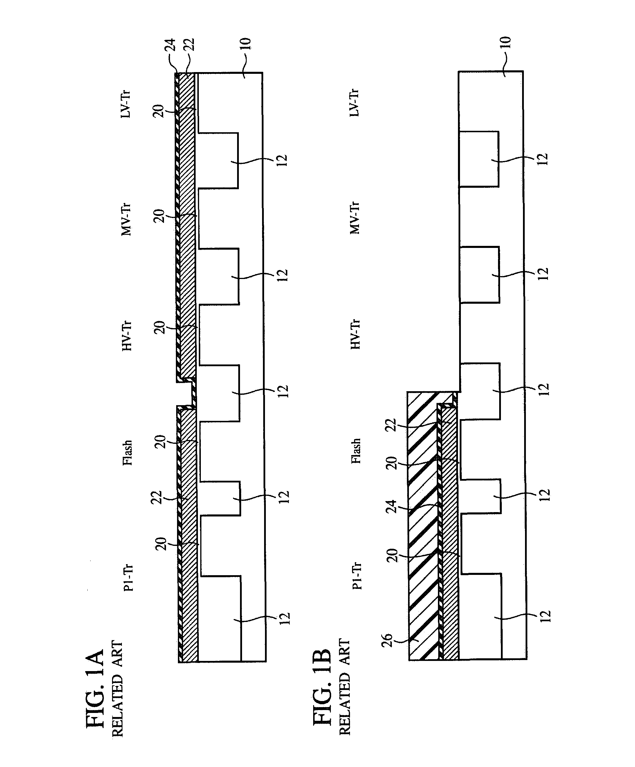
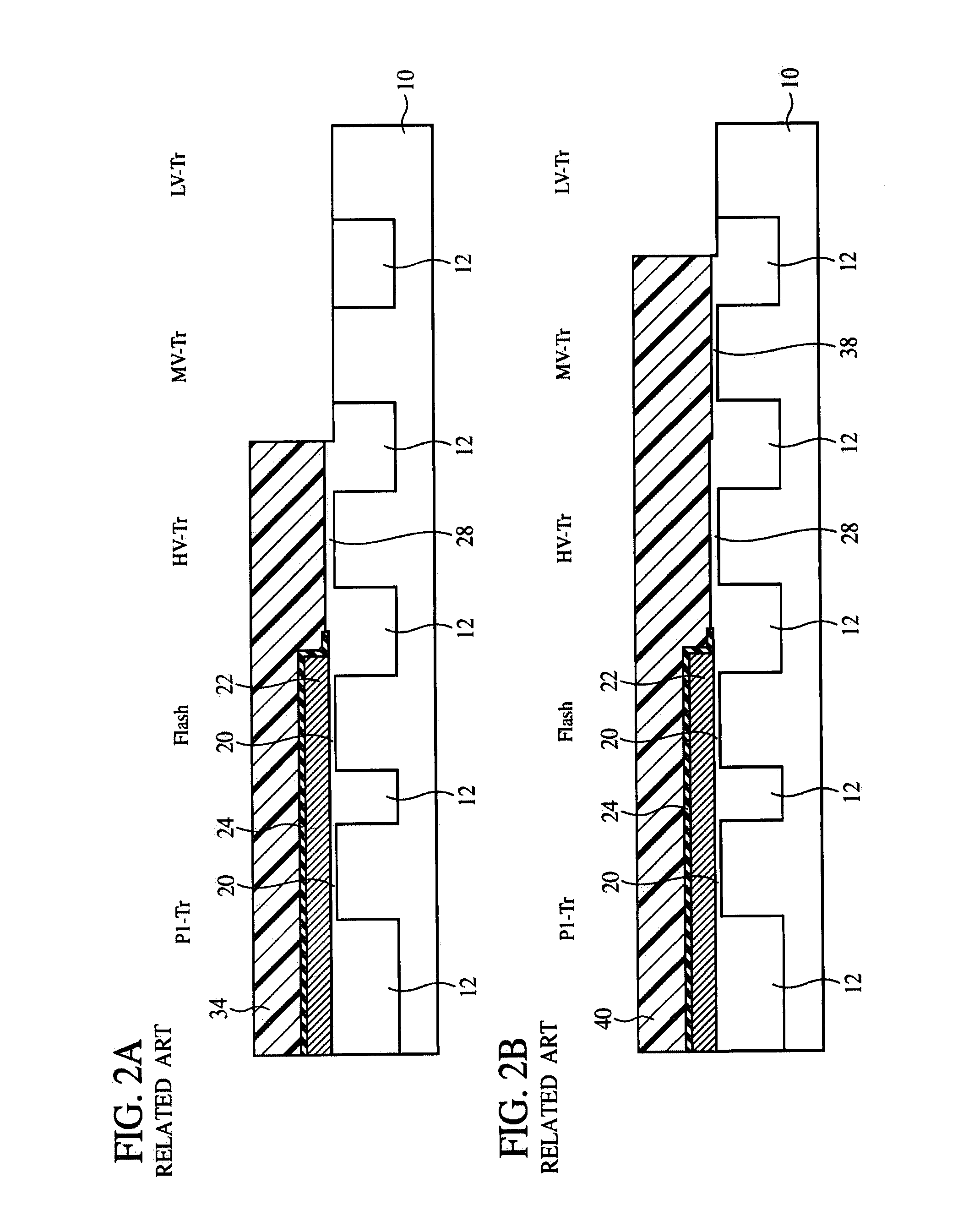
[0029]The method for fabricating the semiconductor device according to a first reference embodiment of the present invention will be explained with reference to FIGS. 1A to 4B. FIGS. 1A to 4B are sectional views showing the steps of the method for fabricating the semiconductor device according to the present embodiment.

[0030]First, a device isolation film 12 for defining device regions is formed in a silicon substrate 10 by, e.g., STI (Shallow Trench Isolation) method. The device regions defined by the device isolation film 12 are, sequentially from the right side of the drawing, a low-voltage transistor (LV-Tr) region, a medium-voltage transistor (MV-Tr) region, a high-voltage transistor (HV-Tr) region, a nonvolatile memory transistor (Flash) region and a Poly-1 transistor (P1-Tr) region. For the details of the respective transistor, refer to the embodiments which will be described later.

[0031]Then, the silicon substrate 10 is thermally oxidized by, e.g....

second reference embodiment

A Second Reference Embodiment

[0059]The method for fabricating the semiconductor device according to a second reference embodiment of the present invention will be explained with reference to FIGS. 5A to 7B. FIGS. 5A to 7B are sectional views showing the steps of the method for fabricating the semiconductor device according to the present embodiment.

[0060]First, a device isolation film 12 for defining device regions is formed in a silicon substrate 10 by, e.g., STI (Shallow Trench Isolation) method. The device regions defined by the device isolation film 12 are, sequentially from the right side of the drawing, a low-voltage transistor (LV-Tr) region, a medium-voltage transistor (MV-Tr) region, a high-voltage transistor (HV-Tr) region, a nonvolatile memory transistor (Flash) region and a Poly-1 transistor (P1-Tr) region. For the details of the respective transistor, refer to the embodiments which will be described later.

[0061]Then, the silicon substrate 10 is thermally oxidized by, e....

first embodiment

A First Embodiment

[0090]The semiconductor device and the method for fabricating the same according to a first embodiment of the present invention will be explained with reference to FIGS. 8 to 16.

[0091]FIG. 8 is a plan view showing a structure of the semiconductor device according to the present embodiment. FIG. 9 is a diagrammatic sectional view showing a structure of the semiconductor device according to the present embodiment. FIGS. 10A-16 are sectional views showing the steps of the method for fabricating the semiconductor device according to the present embodiment.

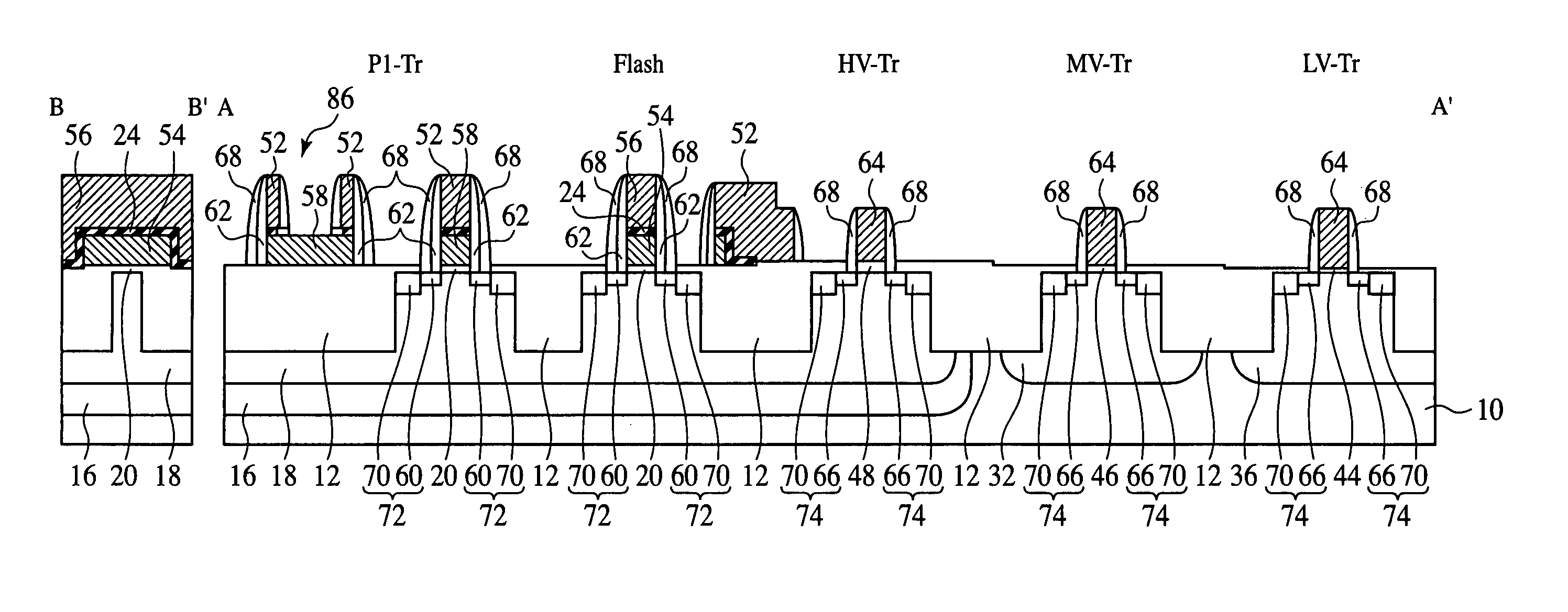
[0092]First, the structure of the semiconductor device according to the present embodiment will be explained with reference to FIGS. 8 and 9.

[0093]FIG. 8 shows a plan view of the typical transistors of logic semiconductor device combined with flash memory. FIG. 9 is the diagrammatic sectional view along the line A-A′ and line B-B′ in FIG. 8.

[0094]The respective transistors are, from the right side of FIG. 8 and FIG. 9...


PUM


Abstract

The method for fabricating the semiconductor device includes the steps of: forming an insulating film 20, a conductive film 22 and an insulating film 24 over a semiconductor substrate 10 having a first to a third region; removing an insulating film 24, the conductive film 22 and an insulating film 20 formed in the second region and the third region; forming an insulating film 38 in the second region and the third region; removing the insulating film 24 in the first region and the insulating film 38 in the third region; forming an insulating film 44 in the third region; after a conductive film 52 has been formed, patterning the conductive films 22, 52 in the first region to form a gate electrode 58; and patterning the conductive film 52 to form gate electrodes 62 in the second region and the third region while removing the conductive film 52 over the gate electrode 58.

Description

CROSS-REFERENCE TO RELATED APPLICATIONS[0001]This application is based upon and claims the benefit of priority from the prior Japanese Patent Application No. 2006-164418, filed on Jun. 14, 2006, the entire contents of which are incorporated herein by reference.BACKGROUND OF THE INVENTION[0002]The present invention relates to a method for fabricating a semiconductor device, more specifically, a method for fabricating a logic semiconductor device combined with a non-volatile memory.[0003]The nonvolatile semiconductor memory cell, such as the flash memory, etc., includes a floating gate for accumulating charges in addition to a control gate for driving the transistor. The floating gate is an electrode which is electrically floating and requires no interconnection to be electrically connected thereto.[0004]However, often an interconnection is electrically connected to a conductive layer which is simultaneously formed with and formed in the same interconnection level as the floating gate...

Claims


Application Information

Patent Timeline
Patent Type & Authority Patents(United States)
IPC IPC(8): H01L21/336
CPCH01L21/823462H01L21/823857H01L27/1052H01L27/11526H01L27/11546H01L27/105H10B99/00H10B41/49H10B41/40
Inventor OGAWA, HIROYUKIKOJIMA, HIDEYUKI
Owner FUJITSU SEMICON LTD
Why Eureka
Try Eureka