Methods and apparatus for cleaning edges of a substrate

Inactive Publication Date: 2007-08-23
SEMITOOL INC
View PDF21 Cites 2 Cited by
  • Summary
  • Abstract
  • Description
  • Claims
  • Application Information

AI Technical Summary

Benefits of technology

[0004] New cleaning apparatus and methods provide significantly better results with difficult to remove contaminants. The contaminants can now be more quickly and easily removed using lower cost and more environmentally friendly cleaning solutions. In one aspect, the cleaning liquid is sprayed or jetted in a direction ge

Problems solved by technology

Even microscopic particles can cause defects and failures in devices.
These types of contaminants can be difficult to completely remove.
Some contaminants are only minimally soluble with preferred aqueous cleaning solutions.
Other contaminants become tightly bonded to an underlying layer on the wafer an

Method used


Image

  • Methods and apparatus for cleaning edges of a substrate
  • Methods and apparatus for cleaning edges of a substrate
  • Methods and apparatus for cleaning edges of a substrate

Examples


Example

DETAILED DESCRIPTION OF THE DRAWINGS

[0019] The invention is directed to apparatus and methods for processing or cleaning a workpiece, such as a semiconductor wafer. The term workpiece or wafer here means any flat article, including semiconductor wafers and other substrates such as glass, mask, and optical or memory media, MEMS substrates, or any other workpiece having, or on which, microelectronic, micromechanical, microelectro-mechanical or micro-optical devices can be formed. The term contaminant here means any unwanted particles, film or other material on a wafer.

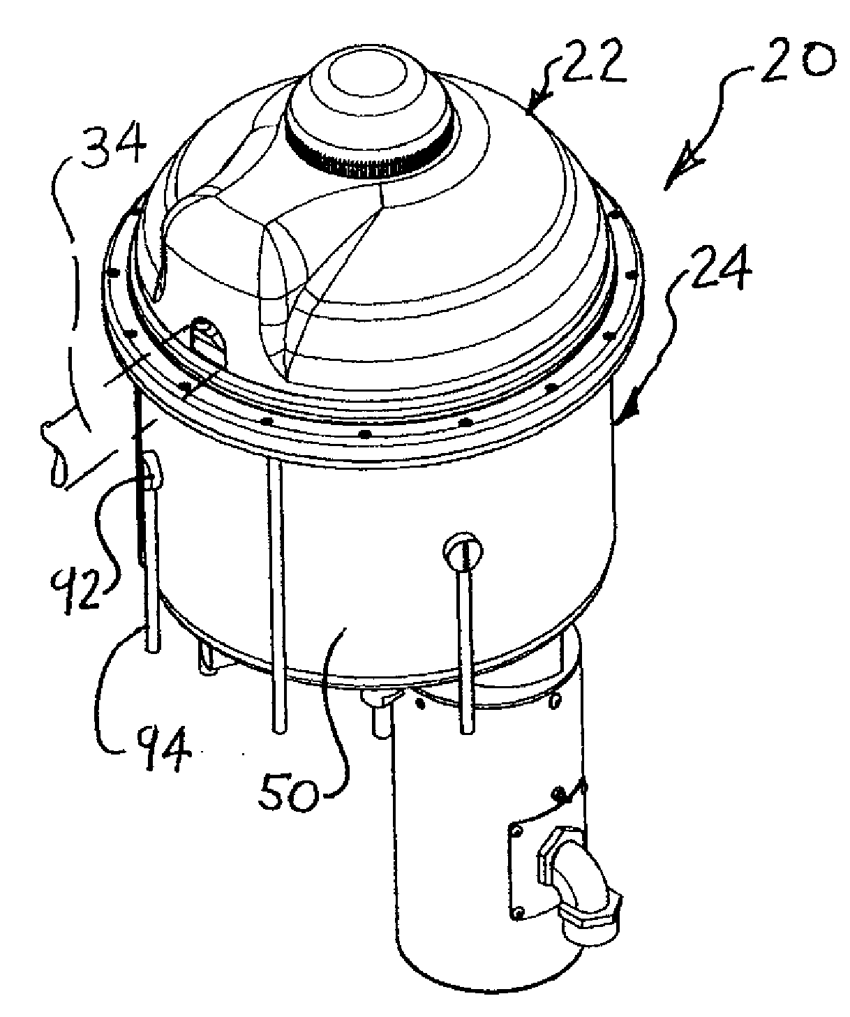
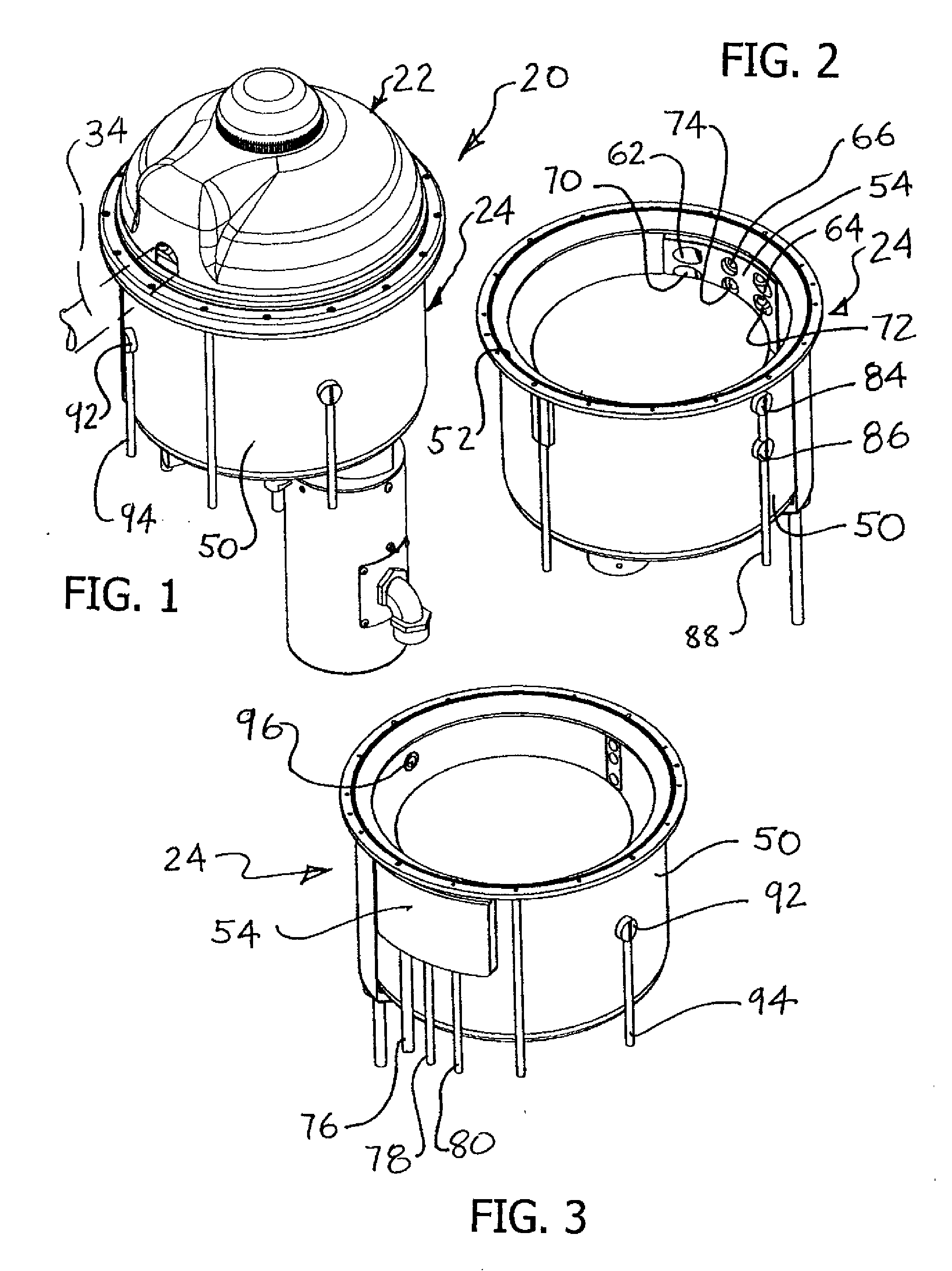
[0020] Turning now to FIGS. 1-3, a processor 20 has a head 22 which may be moved into and out of engagement with a base 24. The base 24 includes a bowl 50 which may have generally cylindrical side walls.

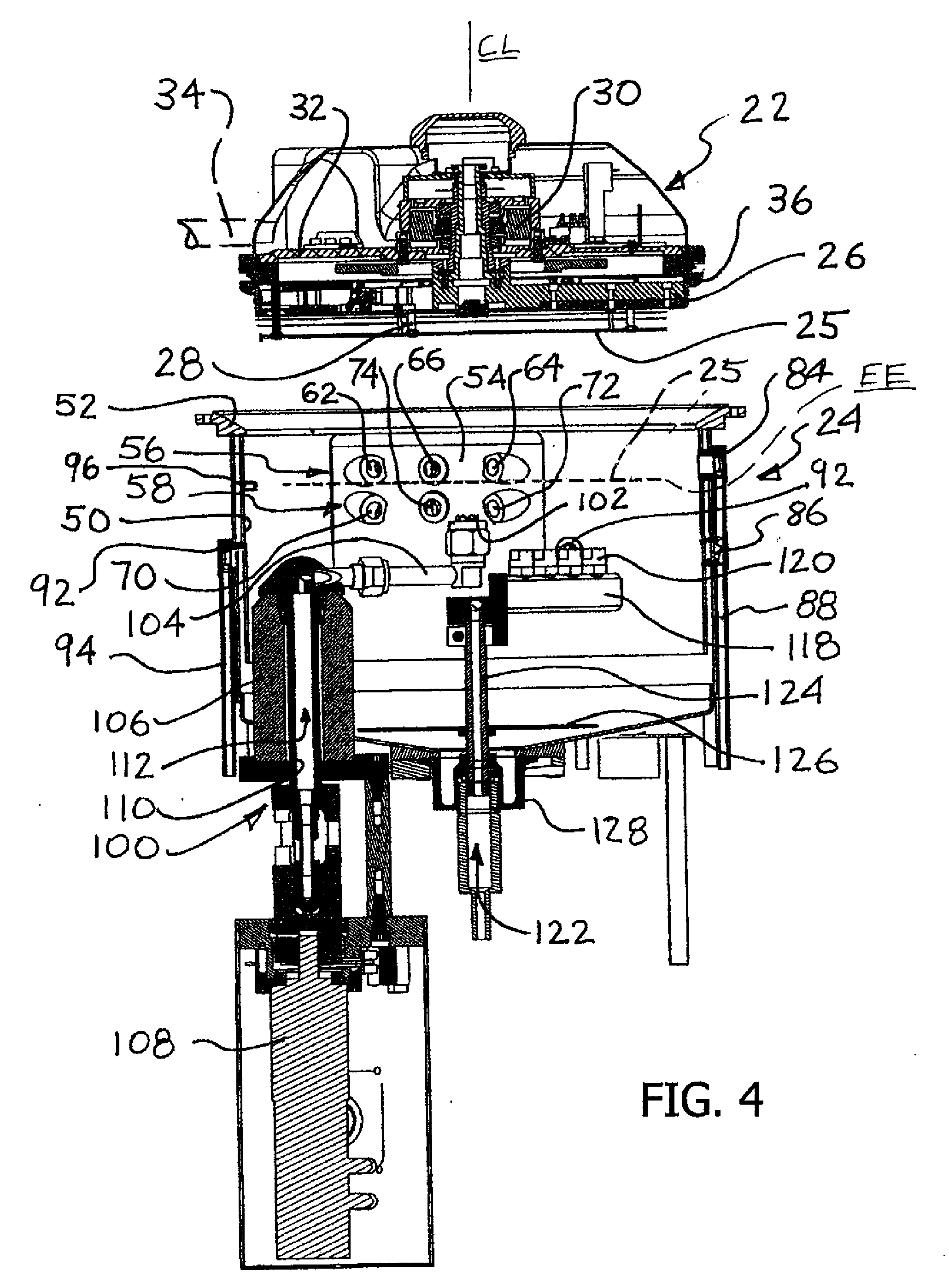
[0021] Turning to FIG. 4, the head 22 typically includes a rotor 26 rotatably supported by a head frame 32. A motor 30 in the head 22 is adapted to spin the rotor 26. Fingers or retainers 28 on the rotor 26 hold a wafe...


PUM

PropertyMeasurementUnit
Temperatureaaaaaaaaaa
Pressureaaaaaaaaaa

Abstract

In methods and apparatus for cleaning a wafer, a cleaning liquid is sprayed or jetted in a direction generally tangent to the circular edge of a spinning wafer. This enhances removal of contaminants from areas near the edge. Re-deposition of contaminant pieces or particles back onto the wafer is reduced because the direction of the spray carries the contaminant off of the wafer. Insoluble contaminant films, such as post etch residue, may be removed via one or more of the pressure of the cleaning liquid, the effects of higher process temperatures from heating the cleaning liquid, and by the chemical composition of the cleaning liquid.

Description

PRIORITY CLAIM [0001] This Application is a continuation-in-part of U.S. patent application Ser. No. 11 / 359,969, filed Feb. 21, 2006 and now pending and incorporated herein by reference.BACKGROUND [0002] Remarkable progress made in microelectronic devices over the past several years has led to more useful yet less expensive electronic products of all types. It has also led to entirely new types of products. A major factor in the development of microelectronic devices has been the machines and methods used to manufacture them. Manufacturing of microelectronic devices requires extreme precision, extremely pure materials, and an extremely clean manufacturing environment. Even microscopic particles can cause defects and failures in devices. [0003] Microelectronic devices are typically manufactured by selectively applying and removing various layers or films of material onto a substrate, such as a silicon wafer. Manufacturing by-products, such as polymer, post etch plasma residue, and ot...

Claims


Application Information

Patent Timeline
IPC IPC(8): C23G1/00B08B3/00B08B7/00
CPCC23G5/00H01L21/67051H01L21/02052
Inventor GHEKIERE, JOHNARVIDSON, AARON W.FENDER, BRUCEMEUCHEL, CRAIG P.SCHRODER, RAOULAEGERTER, BRIANFLINK, RONRYE, JASON
Owner SEMITOOL INC
Why Eureka
Try Eureka