Supercharge Your Innovation With Domain-Expert AI Agents!

276-pin buffered memory module with enhanced fault tolerance

a buffer memory module and fault tolerance technology, applied in the field of buffer memory modules with enhanced fault tolerance, can solve the problem of inherent limits on the number of modules that may be attached to the stub bus

Active Publication Date: 2007-08-23
INT BUSINESS MASCH CORP
View PDF77 Cites 8 Cited by
  • Summary
  • Abstract
  • Description
  • Claims
  • Application Information

AI Technical Summary

Benefits of technology

The solution enables a flexible, high-speed, and reliable memory system architecture that maximizes data rates and minimizes pin count, while maintaining enhanced fault tolerance and error detection / correction capabilities, allowing for efficient communication with both buffered and unbuffered memory modules.

Problems solved by technology

This structure offers a reasonable trade-off between cost, performance, reliability and upgrade capability, but has inherent limits on the number of modules that may be attached to the stub bus.

Method used


Image

  • 276-pin buffered memory module with enhanced fault tolerance
  • 276-pin buffered memory module with enhanced fault tolerance
  • 276-pin buffered memory module with enhanced fault tolerance

Examples


Embodiment Construction

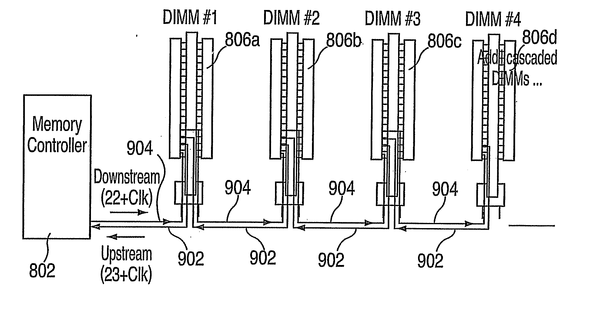
[0032] Exemplary embodiments of the present invention include a flexible, high-speed and high reliability memory system architecture and interconnect structure that includes a single-ended point-to-point interconnection between any two high-speed communication interfaces. The memory subsystem may be implemented in one of several structures, depending on desired attributes such as reliability, performance, density, space, cost, component re-use and other elements. A bus-to-bus converter chip enables this flexibility through the inclusion of multiple, selectable memory interface modes. This maximizes the flexibility of the system designers in defining optimal solutions for each installation, while minimizing product development costs and maximizing economies of scale through the use of a common device. In addition, exemplary embodiments of the present invention provide a migration path that allows an installation to implement a mix of buffered memory modules and unbuffered and / or regi...


PUM


Abstract

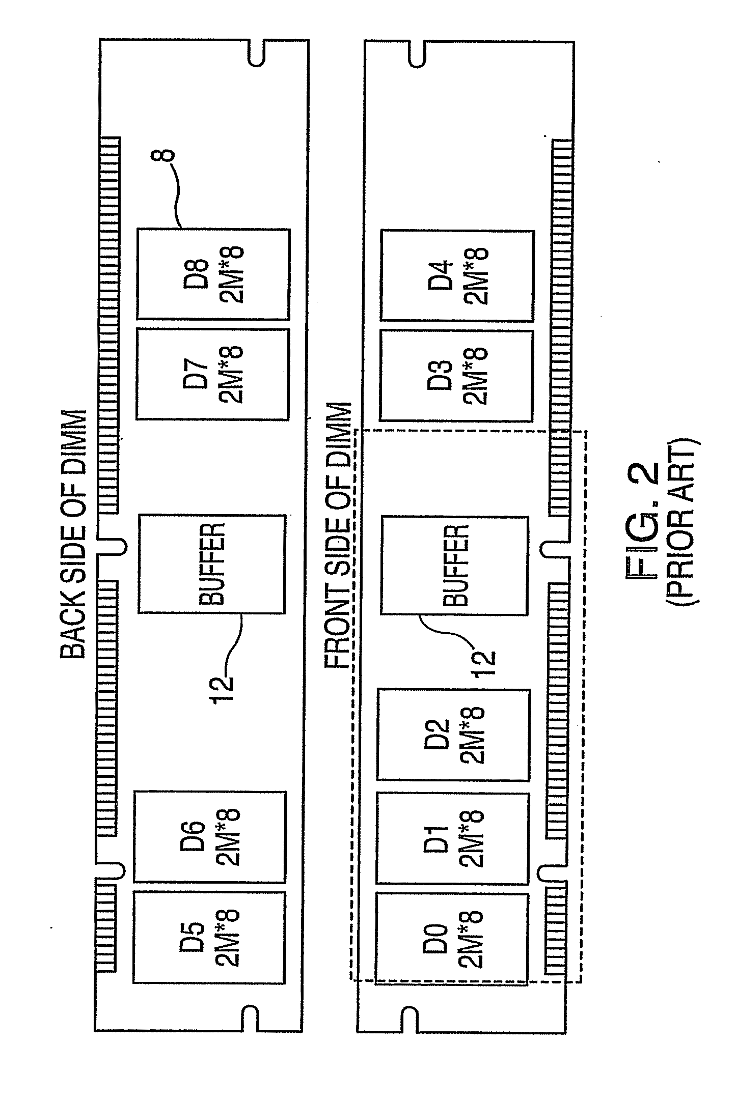
A dual inline memory module (DIMM) includes a card having a length of about 151.2 to about 151.5 millimeters, a pluality of individual local memory devices attached to the card, and a buffer device attached to the card, the buffer device configured for converting a packetized memory interface. The card includes at least 276 pins configured thereon.

Description

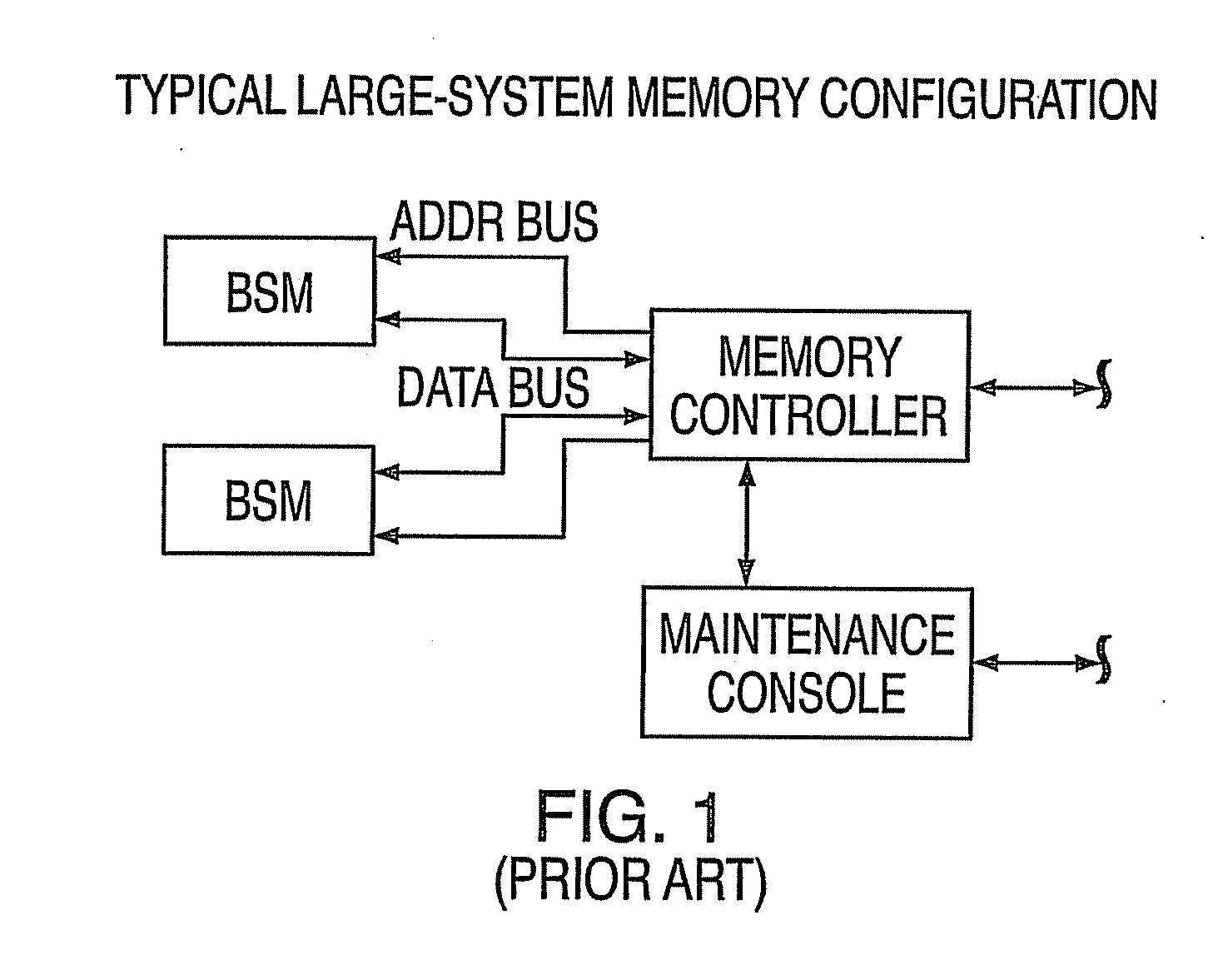
CROSS REFERENCE TO RELATED APPLICATION [0001] This application is a divisional application of U.S. Ser. No. 10 / 903,371 filed Jul. 30, 2004, the contents of which are incorporated by reference herein in their entirety.BACKGROUND OF THE INVENTION [0002] The invention relates to computer memory subsystems and, more particularly, to a buffered memory module having enhanced fault tolerance. [0003] Computer memory subsystems have evolved over the years, but continue to retain many consistent attributes. Computer memory subsystems from the early 1980's, such as the one disclosed in U.S. Pat. No. 4,475,194 to LeVallee et al, of common assignment herewith, included a memory controller, a memory assembly (contemporarily called a basic storage module (BSM) by the inventors) with array devices, buffers, terminators and ancillary timing and control functions, as well as several point-to-point busses to permit each memory assembly to communicate with the memory controller via its own point-to-poi...

Claims


Application Information

Patent Timeline
Patent Type & Authority Applications(United States)
IPC IPC(8): G11C5/06
CPCG11C5/04
Inventor DREPS, DANIELFERRAIOLO, FRANKGOWER, KEVINKELLOGG, MARKRIPPENS, ROGER
Owner INT BUSINESS MASCH CORP
Features
  • R&D
  • Intellectual Property
  • Life Sciences
  • Materials
  • Tech Scout
  • Unparalleled Data Quality
  • Higher Quality Content
  • 60% Fewer Hallucinations
Learn More