Method of manufacturing chip resistors

Inactive Publication Date: 2007-08-23
WALSIN TECHNOLOGY CORPORATION
View PDF8 Cites 0 Cited by
  • Summary
  • Abstract
  • Description
  • Claims
  • Application Information

AI Technical Summary

Benefits of technology

[0022]The main objective of the invention is to provide a method of manufacturing chip resistors that increases production efficiency and yield.

Problems solved by technology

Therefore, conductivity of the inner electrodes (28) will vary and adversely influence yield due to inconsistent thickness of the inner electrodes (28).
Furthermore, barrel plating yield is low because the chip resistor units (30) tend to stick to each because of static electricity generated during barrel plating.

Method used


Image

  • Method of manufacturing chip resistors
  • Method of manufacturing chip resistors
  • Method of manufacturing chip resistors

Examples


Embodiment Construction

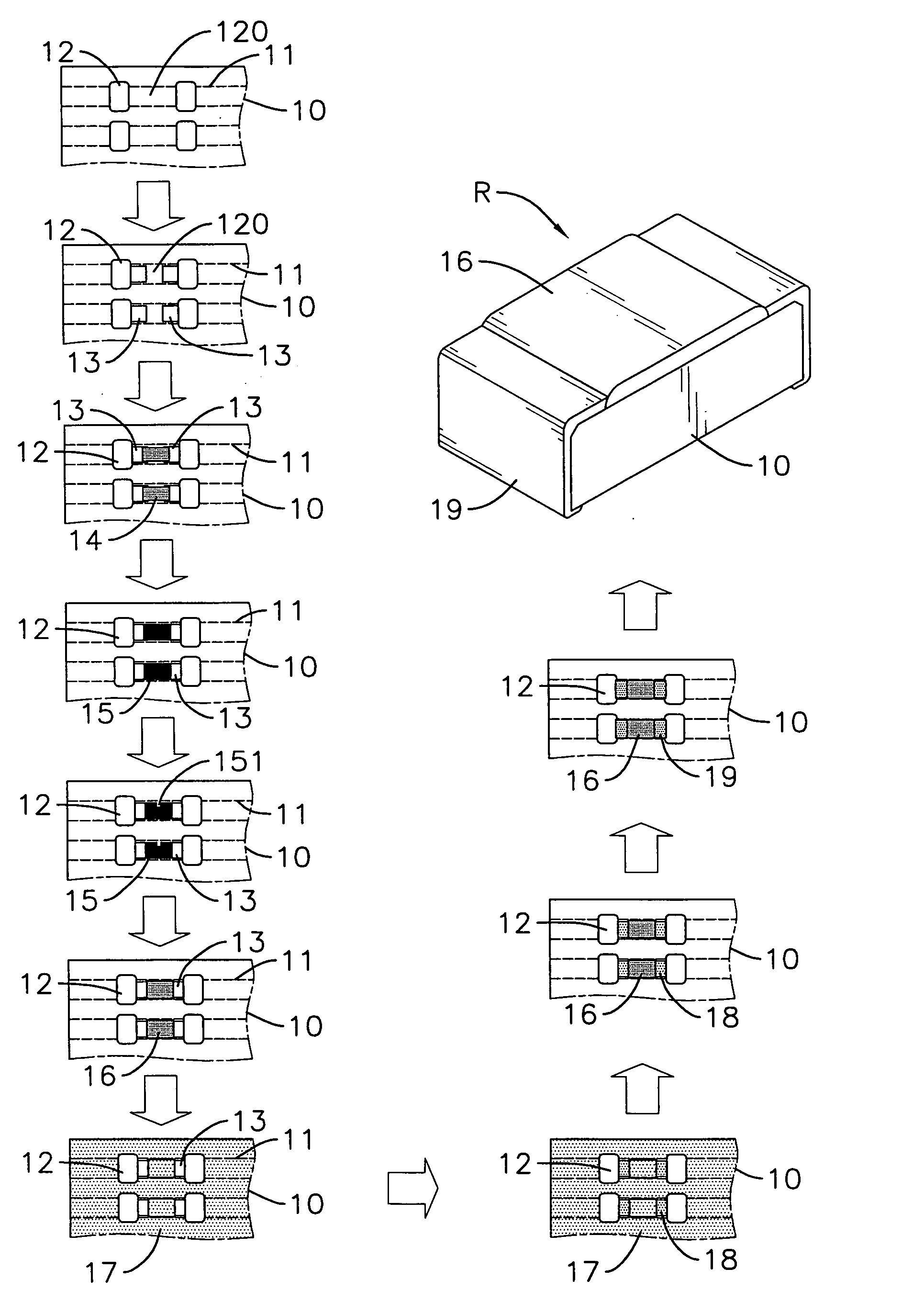
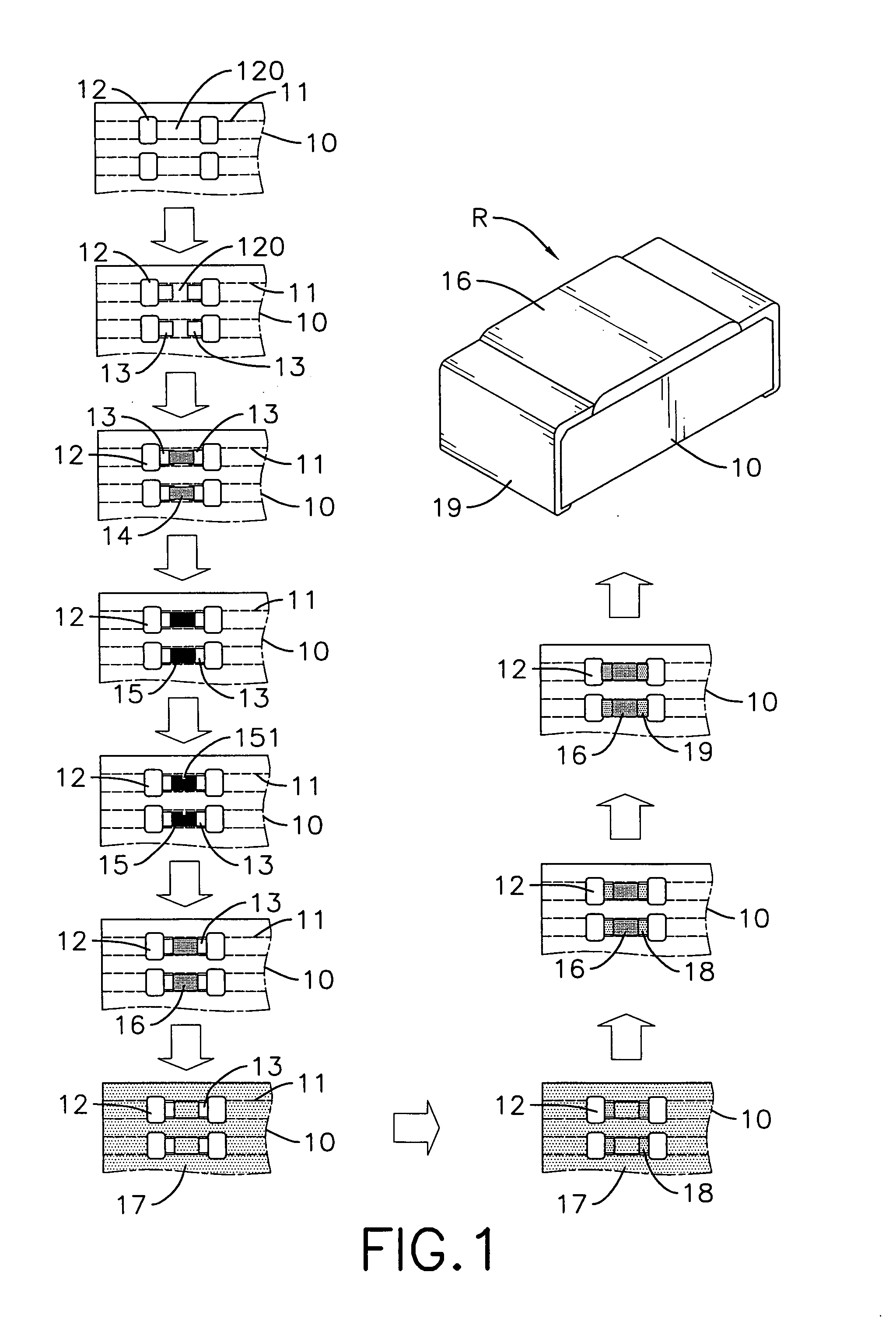
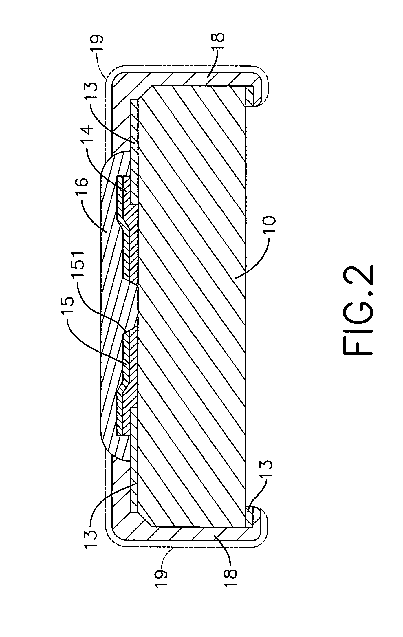
[0029]With reference to FIG. 1, a method of manufacturing chip resistors in accordance with the present invention comprises steps of cutting grooves (11) in a substrate (10), forming through holes (12), defining chip regions (120), forming main electrodes (13), forming resistor layers (14), forming first protective layers (15), optionally adjusting resistance, optionally forming second protective layers (16), forming stripped protective layers (17), forming inner electrodes (18), removing the stripped protective layers (17), plating outer electrodes (19) and cutting the substrate (10).

[0030]The step of cutting grooves (11) in a substrate (10) may be performed with a blade and comprises cutting multiple grooves (11) parallel to each other in a substrate (10). The substrate (10) has a thickness, a top surface and a bottom surface. Each groove (11) has a depth, and the depth of each groove (11) may not be deeper than half the thickness of the substrate (10).

[0031]The step of forming th...


PUM


Abstract

A method of manufacturing chip resistors has steps of cutting grooves in a substrate, forming through holes, defining chip regions, forming main electrodes, forming resistor layers, forming first protective layers, forming stripped protective layers, forming inner electrodes, removing the stripped protective layers, plating outer electrodes and cutting the substrate. The step of cutting grooves on a substrate includes forming multiple parallel grooves on a substrate. The step of forming through holes includes forming multiple through holes between and across two adjacent grooves on the substrate, and each through hole has smooth inner walls. The step of plating outer electrodes includes plating outer electrodes on the inner electrodes by rack plating. The step of cutting the substrate includes cutting the substrate along the grooves to obtain individual chip resistors.

Description

BACKGROUND OF THE INVENTION[0001]1. Field of the Invention[0002]The present invention relates to a method of manufacturing chip resistors, and more particularly to a method of manufacturing chip resistors that increases the production efficiency and yield.[0003]2. Description of Related Art[0004]Because electronic products are becoming smaller, individual active and passive electronic elements have to become smaller, too. For example, standard chip resistors may be 0.60 mm long, 0.30 mm wide and 0.23 mm deep or 0.40 mm long, 0.20 mm wide and 0.23 mm deep. Smaller elements have smaller tolerances for error.[0005]With reference to FIG. 3, a conventional manufacturing method comprises steps of cutting grooves (21, 22) on a substrate (20), defining chip regions (23), forming main electrodes (24), forming resistor layers (25), forming inner protective layers (26), adjusting resistance, forming outer protective layers (27), dividing the substrate (20) into multiple strips (20′), forming i...

Claims


Application Information

Patent Timeline
IPC IPC(8): H01L21/30
CPCH01C1/148H01C17/006H01C7/003
Inventor LUH, SHIOW-CHANGKUO, CHUN-HSIUNG
Owner WALSIN TECHNOLOGY CORPORATION
Why Eureka
Try Eureka