

Optical transceiver PCB mounting system having EMI containment features
- Summary
- Abstract
- Description
- Claims
- Application Information
AI Technical Summary
Benefits of technology
Problems solved by technology
Method used
Image

Examples
Embodiment Construction
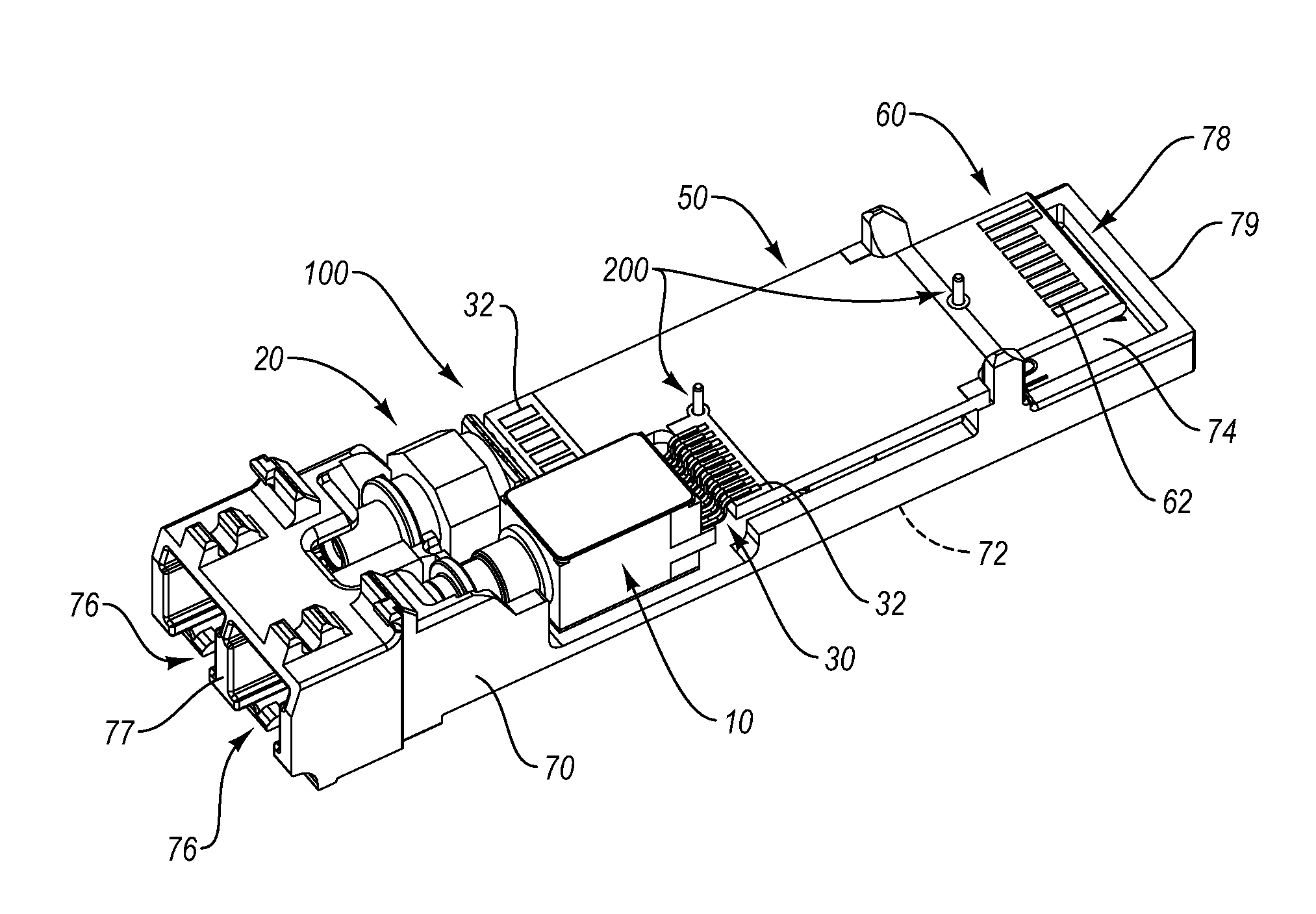
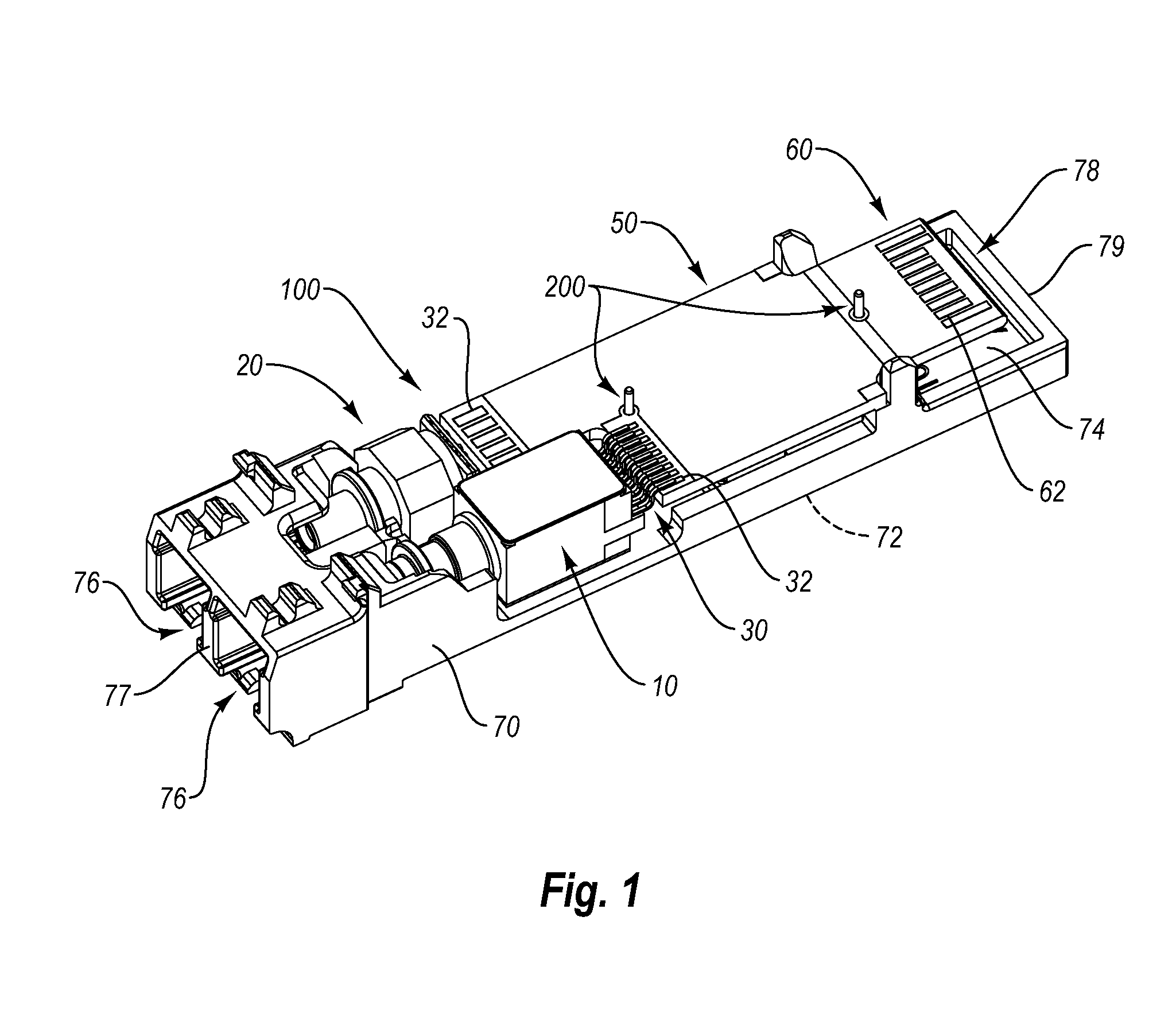
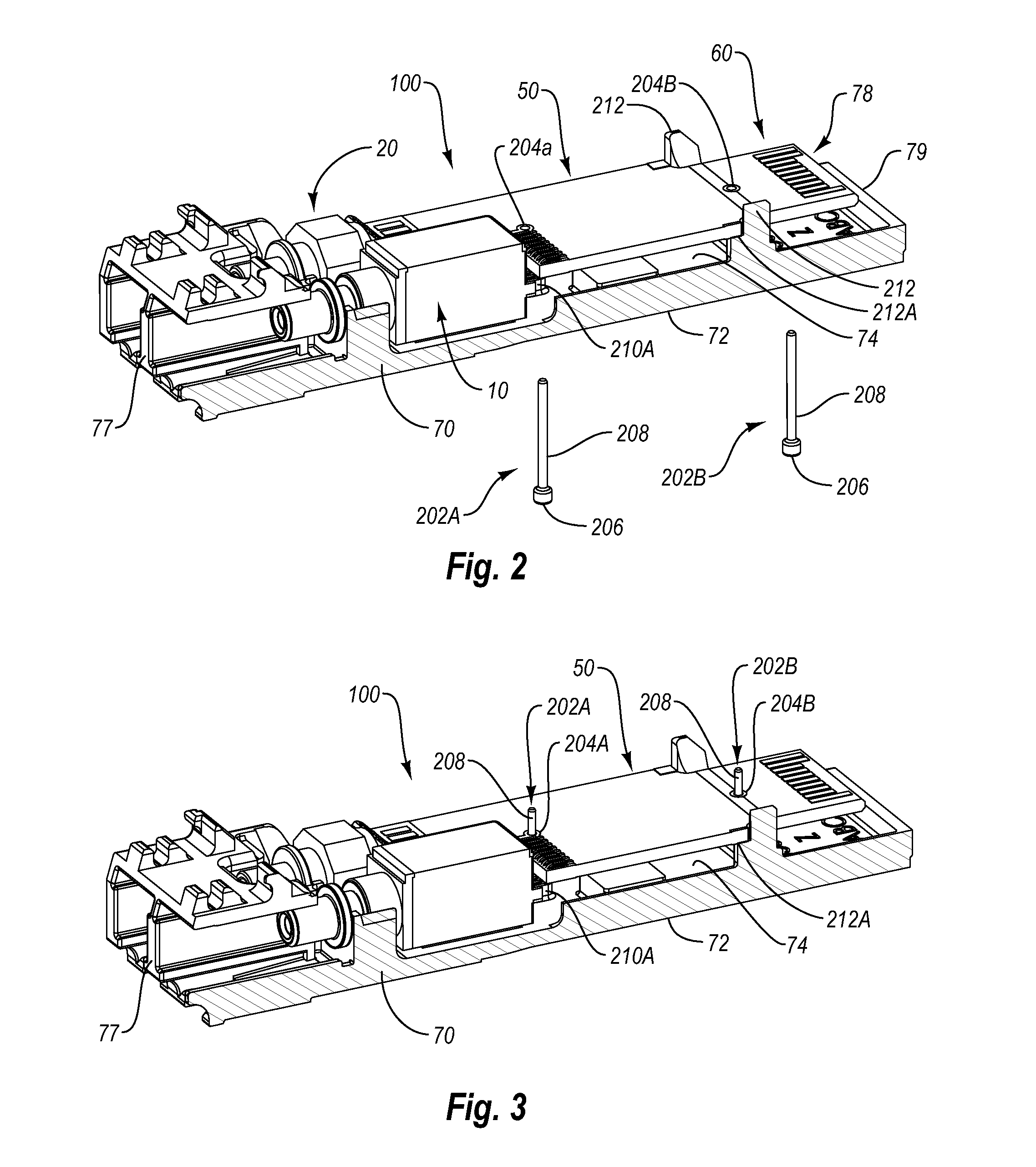
[0025] Reference will now be made to figures wherein like structures will be provided with like reference designations. It is understood that the drawings are diagrammatic and schematic representations of exemplary embodiments of the invention, and are not limiting of the present invention nor are they necessarily drawn to scale.
[0026]FIGS. 1-8 depict various features of embodiments of the present invention, which is generally directed to an optoelectronic device, such as an optical transceiver module, having a printed circuit board, and a mounting system for securing the printed circuit board within the transceiver module. The mounting system minimizes the amount of surface area it occupies on the printed circuit board, thereby preserving relatively more space for critical component placement on the board surface. In addition, the mounting system desirably controls the emission of electromagnetic interference from the transceiver module, thereby reducing signal interference during...
PUM
 Abstract
Description
Claims
Application Information