
Digital/analog conversion circuit

Inactive Publication Date: 2007-09-20
SONY CORP
View PDF1 Cites 4 Cited by
  • Summary
  • Abstract
  • Description
  • Claims
  • Application Information

AI Technical Summary

Benefits of technology

[0037] Therefore, it is desirable to provide a cyclic digital / analog conversion circuit which can reduce a conversion error caused by a mismatch in electrostatic capacitance between capacitors.
[0040] With the digital / analog conversion circuit, the conversion error caused by a mismatch in electrostatic capacitance between capacitors used therein can be reduced.

Problems solved by technology

However, the increase of the ENOB by the correction sequence is restricted by a plurality of factors.
However, this in turn increases the number of times of repetition of the correction sequence, resulting a disadvantage that increased time may be required for correction of the capacitance mismatch.
A more significant problem is that, as the value of the very small capacitor to be added becomes lower, the detection accuracy of the capacitance mismatch has to be raised.
In other words, the correction accuracy of the capacitance mismatch is limited by the accuracy of a detector for the capacitance mismatch such as, for example, a voltage comparator.
This makes a significant factor which obstructs increase of the ENOB.
However, this technique has two problems.
A first one of the problems resides in that the DAC operates in accordance with the dynamic sequence wherein a capacitor is selected for each input bit.
This significantly complicates a circuit for the switching control and besides gives rise to a secondary problem of charge injection and so forth.
The second problem is that an average error is reduced by the technique.
In other words, even where the technique of Non-Patent Document 2 is used, the ENOB may not be improved because the maximum value of the error of the output voltage is same as that by existing techniques.

Method used


Image

  • Digital/analog conversion circuit
  • Digital/analog conversion circuit
  • Digital/analog conversion circuit

Examples


Embodiment Construction

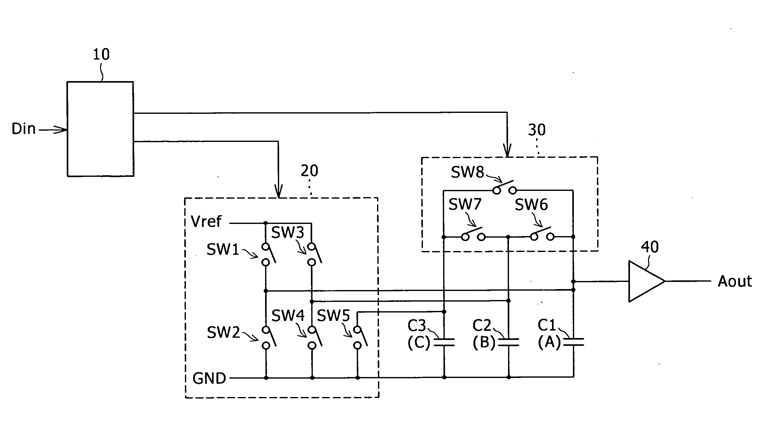
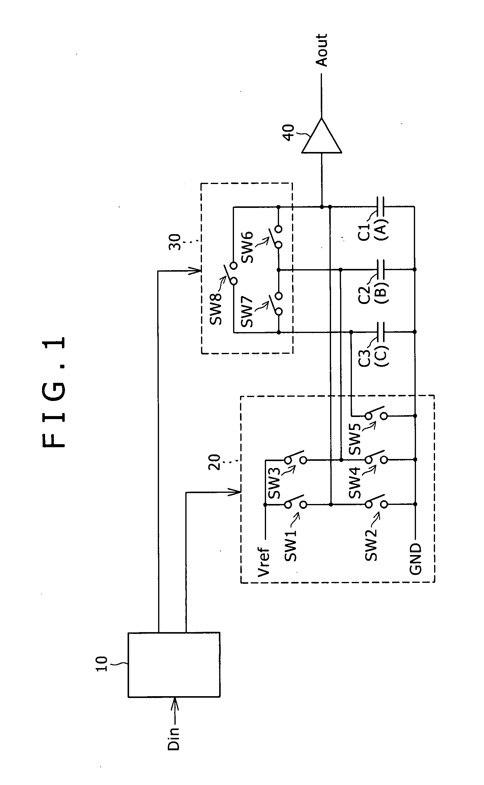
[0060] Referring to FIG. 1, there is shown an example of a configuration of a digital / analog conversion circuit to which the present invention is applied.

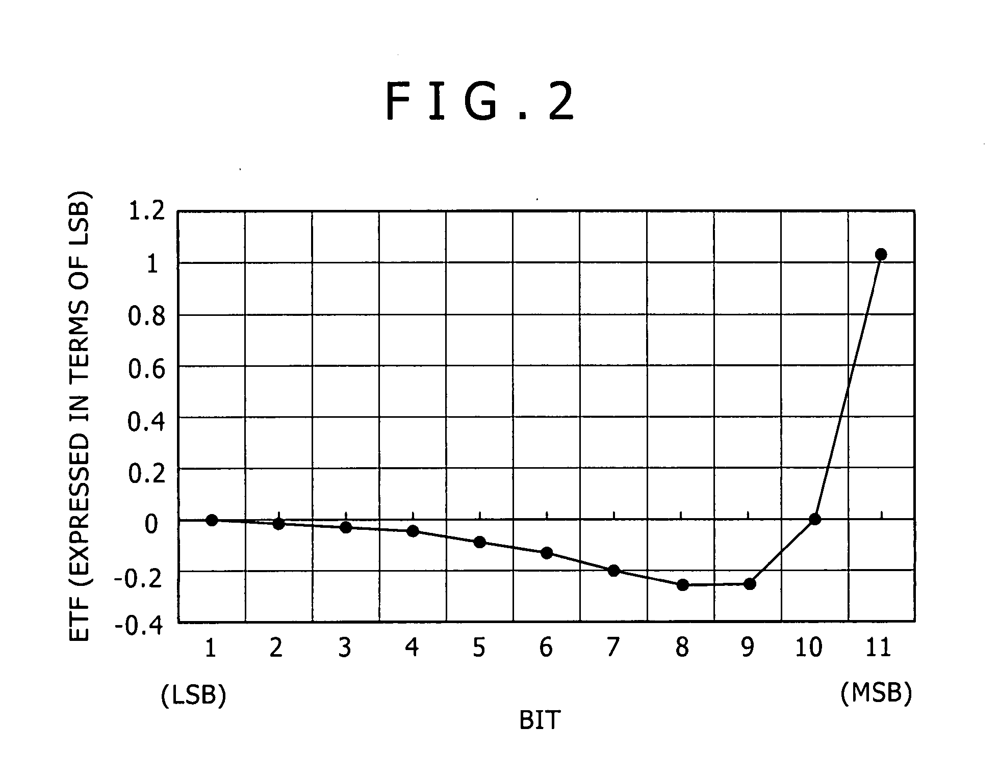
[0061] Before the digital / analog conversion circuit shown in FIG. 1 is described, description is given of a characteristic of an error which occurs with a general cyclic DAC, an outline of a method of reducing the error and a flow diagram useful to understanding of an operation of the cyclic DAC. It is to be noted that, while the following description is given particularly of a cyclic DAC of 11 bits as an example, the present invention can be applied to a cyclic DAC of any bit number and does not rely upon the number of bits.

[0062] First, an error characteristic of a basic cyclic DAC shown in FIG. 13 is studied. In order to recognize the characteristic, an error transfer function (hereinafter referred to in abbreviation as ETF) E(k) is defined as given by the following expression (5): E⁡(k)≡∂Δ⁢ ⁢Vout∂Dk=(1+x)L-k(2+x)L-k+1-12L-k+...


PUM


Abstract

A digital / analog conversion circuit includes a plurality of capacitors, a voltage application section, a connection section, and a control section. The control section is operable to perform the charge sharing operation and to collect the charge supplied from the voltage application section. The control section sets, for at least M higher order ones of the digits of the binary code, the number of times by which the one capacitor takes part in the charge sharing operation within a series of operations before the charge supplied from the voltage application section by the voltage application operation is shared by the last charge sharing operation to twice the number of times by which the one capacitor takes part in the voltage application operation or the charge retaining operation, M being an integer equal to or greater than two.

Description

CROSS REFERENCES TO RELATED APPLICATIONS [0001] The present invention contains subject matter related to Japanese Patent Application JP 2006-052704 filed with the Japanese Patent Office on Feb. 28, 2006, the entire contents of which being incorporated herein by reference. BACKGROUND OF THE INVENTION [0002] 1. Field of the Invention [0003] This invention relates to a digital / analog conversion circuit, and more particularly to a cyclic digital / analog conversion circuit. [0004] 2. Description of the Related Art [0005] A digital / analog converter (hereinafter referred to simply as DAC) is a circuit for converting a digital signal which has been subject to various digital processes into an analog signal so as to be outputted as a real signal, and is one of basic components of electric apparatus. The DAC is used widely in television receivers, audio apparatus, communication apparatus and so forth. In the apparatus mentioned, the DAC is used as a circuit for converting a digital signal whic...

Claims


Application Information

Patent Timeline
IPC IPC(8): H03M1/66
CPCH03M1/667H03M1/0697
Inventor UENO, YOSUKE
Owner SONY CORP
Learn More