Light-Emitting Element and Display Device

a technology of light-emitting elements and display devices, which is applied in the direction of discharge tubes/lamp details, discharge tubes luminescnet screens, electric discharge lamps, etc., can solve the problems of reducing the manufacturing process of elements, reducing the actual use of materials, and reducing so as to reduce the cost, reduce the manufacturing time of elements, and achieve high light-extraction efficiency

Active Publication Date: 2007-09-27
SEMICON ENERGY LAB CO LTD
View PDF16 Cites 40 Cited by
  • Summary
  • Abstract
  • Description
  • Claims
  • Application Information

AI Technical Summary

Benefits of technology

[0022] Further, it is clear that the slight amount of material is needed to be used, and thus the manufacturing time of an element can be shortened, which results in reduction of cost. As described above, various effects can be obtained by forming a part of intermediate conductive layer to be island-like instead of to be film-like as conventionally.
[0023] Further, a display device according to the present invention has a light-emitting element that provides the above described operation effects; therefore various operation effects such as high light-extraction efficiency, low power-consumption, low cost and long life can be obtained.

Problems solved by technology

However, materials that have been used actually are limited to the followings: 1: a stacked layer of a mixed layer containing an electron transporting compound such as Alq or bathocuproin (BCP) and an electron injecting compound such as an alkali metal and a transparent electrode such as ITO (indium tin oxide) or IZO (indium zinc oxide); 2: a stacked layer of the mixed layer containing the electron transporting compound and the electron injecting compound and a metal oxide; 3: a stacked layer of the mixed layer containing the electron transporting compound and the electron injecting compound and an electron-accepting organic compound, and the like.
By using the above described materials, the intermediate conductive layer can keep transparency; however, the material is largely limited and a manufacturing process of an element becomes also complicated.
However, a transparent electrode such as ITO or IZO cannot be formed by a vacuum vapor deposition method and formed by a sputtering method.
Therefore, such transparent electrodes should be formed after an element is transferred into a chamber for forming a film by a sputtering method from a chamber for an evaporation method, and thus the manufacturing process becomes complicated.

Method used


Image

  • Light-Emitting Element and Display Device
  • Light-Emitting Element and Display Device
  • Light-Emitting Element and Display Device

Examples


example 1

[0059] In this example, the structure of an active matrix display device (also referred to as an active matrix light-emitting device) using a light-emitting element according to Embodiment is explained with reference to FIGS. 3A, 3B4A and 4B. A display device according to this example has a plurality of pixels 310 including a plurality of elements in a region formed by the intersection of a source line Sx (x is a natural number, 1≦x≦m) with a gate line Gy (y is a natural number, 1≦x≦n) with an insulator interposed therebetween (FIG. 3A). The pixel 310 has a light-emitting element 313, a capacitor element 316 and two transistors. One of the two transistors is a transistor for switching 311 (switching transistor) for controlling input of a video signal to the pixel 310, and the other is a transistor for driving 312 (driving transistor) for controlling light emission and non-light emission of the light-emitting element 313. The capacitor element 316 serves to hold gate-source voltage o...

example 2

[0092] In this example, an example of a pixel circuit that can be applied to the present invention except the pixel circuit shown in FIG. 3A is explained with reference to FIGS. 5A and 5B. FIG. 5A shows a pixel circuit having a structure in which a transistor 340 for erasing and a gate wiring Ry for erasing are added to the pixel 310 that is shown in FIG. 3A. Since current does not flow to the light-emitting element 313 forcibly by the arrangement of the transistor 340, a lightning period can be started simultaneously with or immediately after starting a writing period without waiting for writing signals into all of pixels 310. Therefore, a duty ratio is improved, and thus a moving image can be especially displayed so well.

[0093]FIG. 5B shows a pixel circuit in which a transistor 312 of the pixel 310 shown in FIG. 3A is omitted and transistors 341, 342, and a power source line Vax (x is a natural number, 1≦x≦1) are provided anew. The power source line Vax is connected to a power so...

example 3

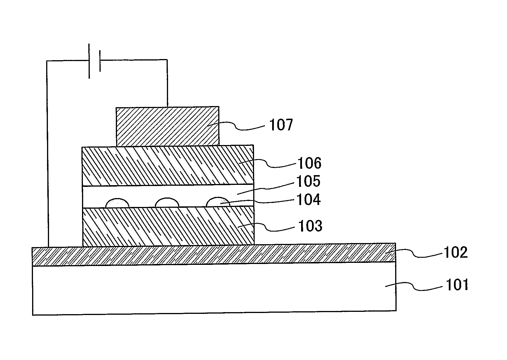
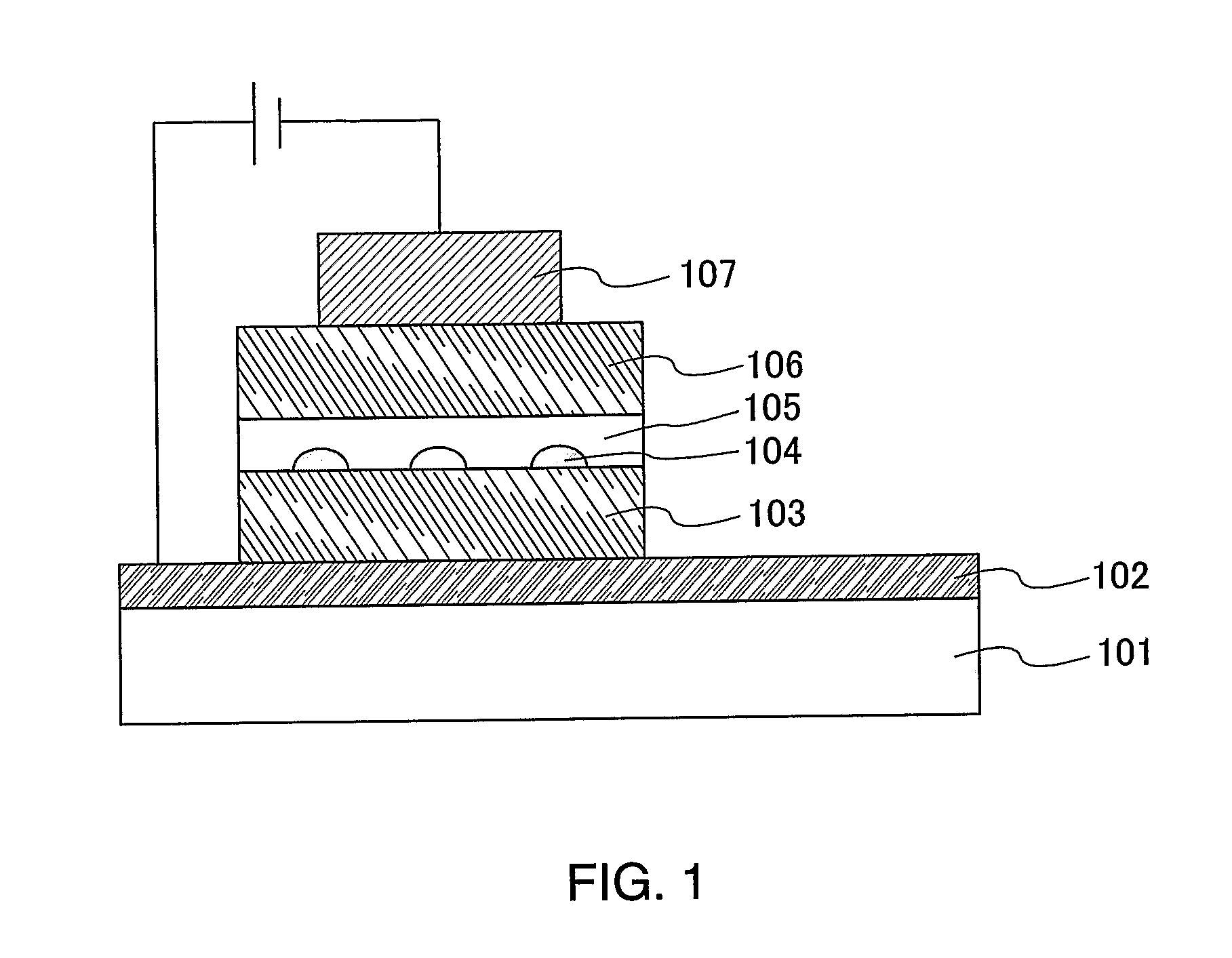
[0094] In this example, stacked layer structures of the wiring 414 (including a second power source 318 through this example) and the pixel electrode (anode or cathode) in the foregoing example are explained with reference to FIGS. 6A to 6D. FIGS. 6A to 6D each show only a part of a light-emitting element of a pixel region. In the FIGS. 6A to 6D, a second light-emitting layer, an intermediate conductive layer and the like are not shown.

[0095]FIG. 6A shows the case that the wiring is formed to have a stacked layer structure of Mo 600 and an alloy containing aluminum 601 and the pixel electrode (e.g., anode 102 through this example) is formed using ITO 602. As the alloy containing aluminum 601, aluminum containing carbon, nickel, cobalt, iron, silicon, or the like is preferably used. It is preferable that the rate of content of carbon is preferably 0.1 to 3.0 atomic %; at least one kind of nickel, cobalt, and iron, 0.5 to 7.0 atomic %; and silicon, 0.5 to 2.0 atomic %. The material h...


PUM


Abstract

When a light-emitting element having an intermediate conductive layer between a plurality of light-emitting layers is formed, the intermediate conductive layer can have transparency; and thus, materials are largely limited and the manufacturing process of an element becomes complicated by a conventional method. A light-emitting element according to the present invention is formed by sequentially stacking a pixel electrode, a first light-emitting layer, an intermediate conductive layer (including an electron injecting layer and a hole-injecting layer, one of which is island-like), a second light-emitting layer and an opposite electrode. Therefore, the present invention can provide a light-emitting element typified by an organic EL element in which arange of choice of materials that can be used as the intermediate conductive layer is broadened extremely, and which can realize a high light-emitting efficiency, a low power consumption and a high reliability, and further a display device using the light-emitting element.

Description

TECHNICAL FIELD [0001] The present invention relates to an element having a structure in which an anode, a cathode, and a thin film sandwiched between the anode and the cathode are formed, and the thin film emits light with a phenomenon called electroluminescence (hereinafter, also referred to as EL) (hereinafter, referred to as a light-emitting element) and to a display device provided with the light-emitting element over a substrate. Further, the present invention relates to an electronic device in which the light-emitting element is provided in an image-display portion. BACKGROUND ART [0002] An EL display is one of light-emitting devices that have attracted most attentions as the next generation flat panel display. In a light-emitting element used for a light-emitting device, a thin film containing an organic compound (hereinafter, referred to as an organic thin film) is formed between two electrodes, and current is applied to the electrodes to generate electroluminescence. Elect...

Claims


Application Information

Patent Timeline
Patent Type & Authority Applications(United States)
IPC IPC(8): H05B33/22H01L27/32H01L51/50H01L51/52H05B33/02H05B33/14
CPCH01L27/3209H01L51/5088H01L51/5092H01L51/5278H01L2924/0002H01L33/42H01L2924/00H10K59/32H10K50/17H10K50/171H10K50/19H10K50/30
Inventor YAMAZAKI, SHUNPEINOMURA, RYOJISEO, SATOSHIABE, HIROKONAKAMURA, YASUO
Owner SEMICON ENERGY LAB CO LTD
Why Eureka
Try Eureka