Light emitting device and manufacturing method thereof

a technology of light-emitting devices and manufacturing methods, which is applied in the direction of semiconductor devices, organic semiconductor devices, electrical devices, etc., can solve the problems of increasing film stress, and achieve the effect of reducing drive voltage and high light-emission efficiency

Inactive Publication Date: 2007-10-04
SEMICON ENERGY LAB CO LTD
View PDF47 Cites 85 Cited by
  • Summary
  • Abstract
  • Description
  • Claims
  • Application Information

AI Technical Summary

Benefits of technology

[0016] An object of the present invention is to extend longevity of a light emitting element having an organic compound.

Problems solved by technology

These inorganic insulating films each have a high blocking effect against moisture; however, as film thickness thereof is increased, a film stress is increased and they tend to be partially peeled or totally removed as a film.

Method used


Image

  • Light emitting device and manufacturing method thereof
  • Light emitting device and manufacturing method thereof
  • Light emitting device and manufacturing method thereof

Examples


embodiment mode 1

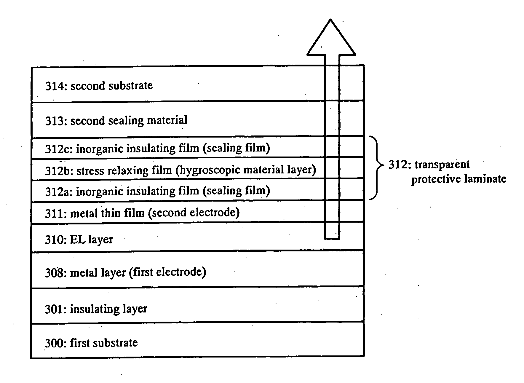
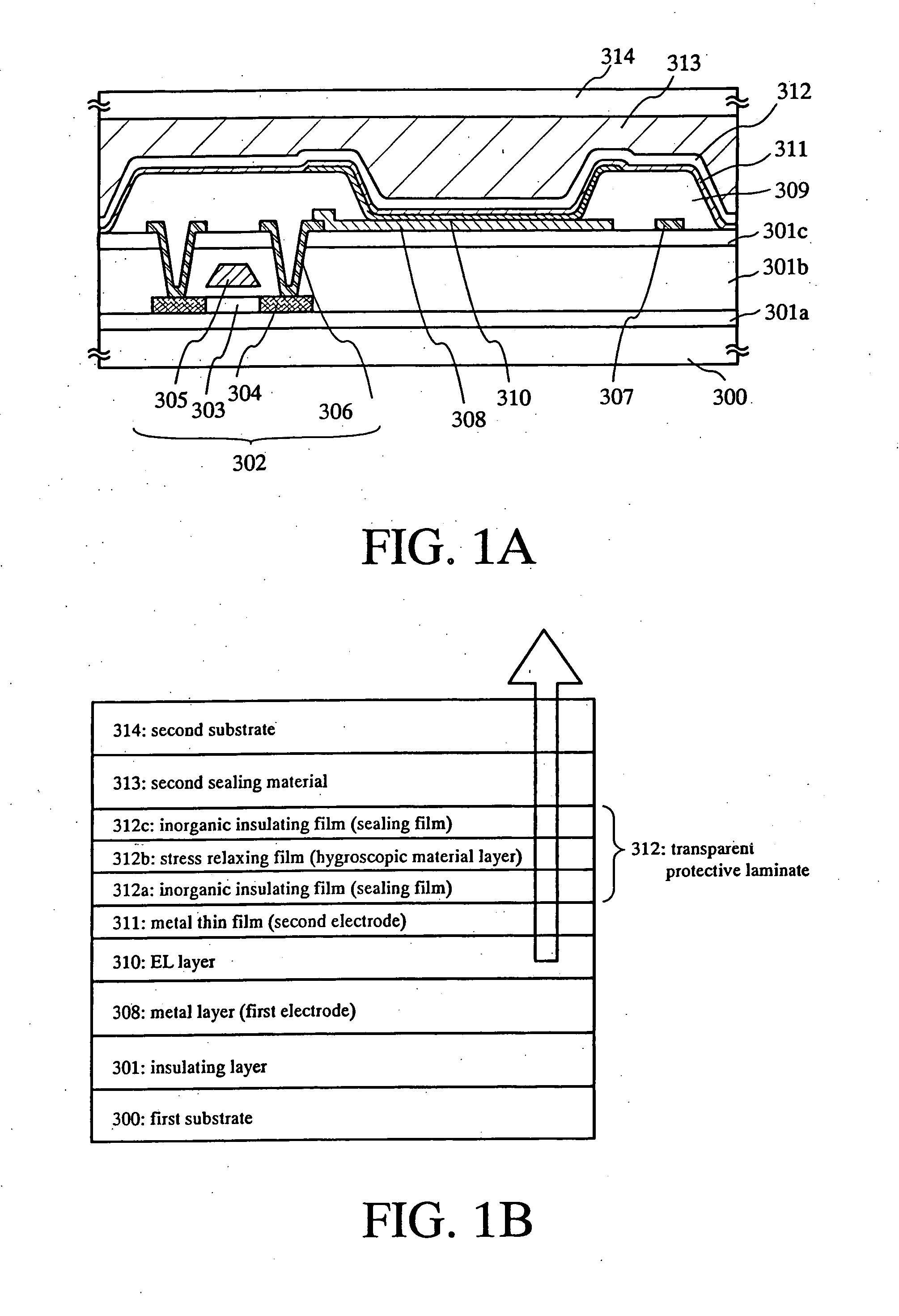
[0063] An top emission type light emitting device according to the invention will be described with reference to FIGS. 1A and 1B.

[0064]FIG. 1A is a cross-sectional view of a part of a pixel portion. FIG. 1B is a simplified view of a laminate constitution in a light emitting region whereupon luminescence is discharged in a direction which an arrow indicates. As for a configuration of light emitting region, namely, a configuration of pixel electrodes, a stripe arrangement, a delta arrangement, a mosaic arrangement and the like are mentioned.

[0065] In FIG. 1A, reference numeral 300 denotes a first substrate; reference numerals 301a, 301b, and 301c each designate insulating layers; reference numeral 302 denotes a TFT; reference numeral 308 denotes a first electrode; reference numeral 309 denotes an insulating material; reference numeral 310 denotes an EL layer; reference numeral 311 denotes a second electrode; reference numeral 312 denotes a transparent protective laminate; reference ...

embodiment mode 2

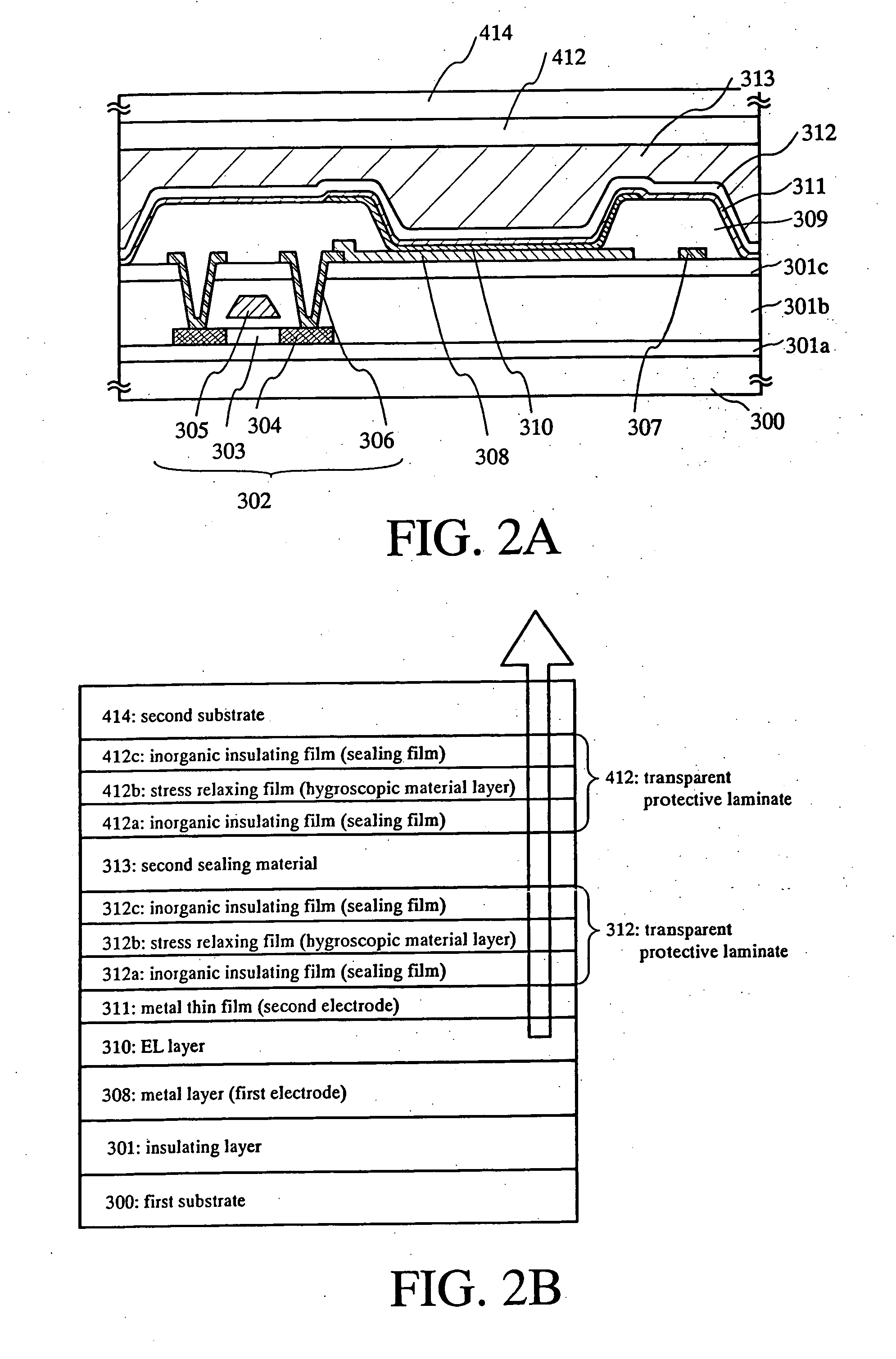
[0081] An example in which a plastic substrate is used as a second substrate and a transparent protective layer is provided over the substrate is shown in FIGS. 2A and 2B. Since the example shown in FIGS. 2A and 2B are constituted in a same manner as in FIGS. 1A and 1B except for the second substrate, same reference numerals are applied to parts identical to those in FIGS. 1A and 1B.

[0082] As for the second substrate 414, a plastic substrate comprising at least one member selected from the group consisting of: polyethylene terephthalate (PET), polyether sulfone (PES), polyethylene naphthalate (PEN), polycarbonate (PC), nylon, polyether etherketone (PEEK), polysulfone (PSF), polyether imide (PEI), polyallylate (PAR), polybutylene terephthalate (PBT), and polyimide may be used.

[0083] A transparent protective laminate 412 similar to the transparent protective laminate 312 as shown in Embodiment Mode 1 is formed over the second substrate 414.

[0084] The transparent protective laminate...

embodiment mode 3

[0087] A bottom emission type light emitting device according to the present invention will be described with reference to FIGS. 3A and 3B.

[0088]FIG. 3A is a view showing a cross-section of a part of a pixel portion. Further, FIG. 3B is a simplified view of a laminate constitution in a light emitting region whereupon luminescence is discharged in a direction which an arrow indicates.

[0089] In FIG. 3A, reference numeral 500 denotes a first substrate; reference numerals 501a, 501b, and 501c each designate an insulating layer; reference numeral 502 denotes a TFT; reference numeral 508 denotes a first electrode; reference numeral 509 denotes an insulating material; reference numeral 510 denotes an EL layer; reference numeral 511 denotes a second electrode; reference numeral 512 denotes a protective laminate; reference numeral 513 denotes a space (inert gas); and reference numeral 514 denotes a second substrate.

[0090] The TFT 502 (p-channel type TFT) provided over the first substrate ...


PUM


Abstract

A light emitting element having an organic compound, which can be extended its longevity is provided. According to the present invention, there is provided a constitution in which, in order to protect a light emitting element from moisture, an inorganic insulating film 312a, a stress relaxation layer 312b having transparency and a hygroscopic property, and an inorganic insulating film 312c are repeatedly laminated over a cathode. The stress relaxation layer 312b having transparency and the hygroscopic property uses at least one film selected from the group consisting of a film comprising a same material as that of a layer 310, containing an organic compound, sandwiched between a cathode and an anode, a layer capable of being formed by vapor deposition, and a layer capable of being formed by coating.

Description

BACKGROUND OF THE INVENTION [0001] 1. Field of the Invention [0002] The present invention relates to a semiconductor device having a circuit comprised of thin film transistor (hereinafter, TFT) and a manufacturing method thereof. For instance, the present invention relates to a light emitting device using a light emitting element which has a film containing an organic compound (hereinafter, organic compound layer) between a pair of electrodes and which can give fluorescence or luminescence by receiving an electric field, and a manufacturing method thereof. The light emitting device referred to in the present specification is an image display device, a light emitting device or a light source (including lighting installation). Additionally, the following are included in examples of the light emitting device: a module wherein a connector, for example, a flexible printed circuit (FPC) or a tape automated bonding (TAB) tape, or a tape carrier package (TCP) is set up onto a light emitting...

Claims


Application Information

Patent Timeline
Patent Type & Authority Applications(United States)
IPC IPC(8): H01L29/04H01L27/15H01L27/32H01L31/12H01L51/52
CPCH01L27/3211H01L2251/5315H01L51/5237H01L27/3244H10K59/35H10K59/12H10K50/846H10K50/8445H10K50/844H10K2102/3026
Inventor YAMAZAKI, SHUNPEITAKAYAMA, TORU
Owner SEMICON ENERGY LAB CO LTD
Why Eureka
Try Eureka