Signal switching device

a signal switching and signal technology, applied in the field of high frequency circuits, can solve the problems of reducing the reliability of mechanical switches, and reducing the loss of signals levels, etc., and achieves the effects of low signal loss, good isolation characteristic, and large impedance of the first transmission path

Inactive Publication Date: 2007-10-04
NTT DOCOMO INC
View PDF6 Cites 0 Cited by
  • Summary
  • Abstract
  • Description
  • Claims
  • Application Information

AI Technical Summary

Benefits of technology

[0009] Accordingly, it is a general object of the present invention to solve one or more problems of the related art by providing a signal switching device capable of transmitting signals with less signal loss while maintaining a good isolation characteristic.
[0010] A more specific object of the present invention is to provide a signal switching device capable of transmitting signals with less signal loss while maintaining a good isolation characteristic without being connected with a switching element such as a mechanical switch or a semiconductor switch.
[0014] According to the present invention, by providing a first section formed by a superconducting material connected to the first transmission path, when switching input signals to the second transmission path, the first section in the first transmission path formed by a superconducting material is set to a non-superconducting state. Because a portion at the input end of the first section has a smaller cross section than that of the output end of the first section, the resistance of the first transmission path becomes very large in the non-superconducting state. Consequently, a good isolation characteristic can be achieved; furthermore, signal loss occurring in the first transmission path can be reduced effectively.
[0021] According to the present invention, by providing a second section formed from a superconducting material on the second transmission path in parallel, it is possible to appropriately control signal transmission to the subsequent circuits connected to the second transmission path without using mechanical switches or semiconductor switches.
[0023] When switching the input signals to the second transmission path, the first section and the second section are both in the non-superconducting state. Therefore, the impedance of the first transmission path is very large, and input signals propagate to the second transmission path with extremely low signal loss to the first transmission path. Further, because the cross section of the second section connected to the second transmission path in parallel is very small, the impedance to the second section is very large, hence the signals propagating in the second transmission path continue to propagate to the circuits connected to the second transmission path with little signals being branched by the second section. Consequently, a good isolation characteristic can be achieved, and signal loss occurring in the either transmission path can be reduced effectively.

Problems solved by technology

However, when the above technique is used to improve the isolation characteristic, degradation of signals entering the desired transmission path and loss of levels of the signals are not always reduced.
The related art cannot meet this requirement.
However, the reliability of a mechanical switch declines due to its switching mechanism.
Although the problem related to the mechanical switch is avoidable by using a semiconductor switch, the isolation characteristic of a semiconductor switch is not as good as that of the mechanical switch.
Further, when using the above switches, appropriate signals for controlling their switching operations have to be generated and devices capable of switching operations according to the control signals have to be configured, making a signal switching device complicated.

Method used


Image

  • Signal switching device
  • Signal switching device
  • Signal switching device

Examples


first embodiment

First Example

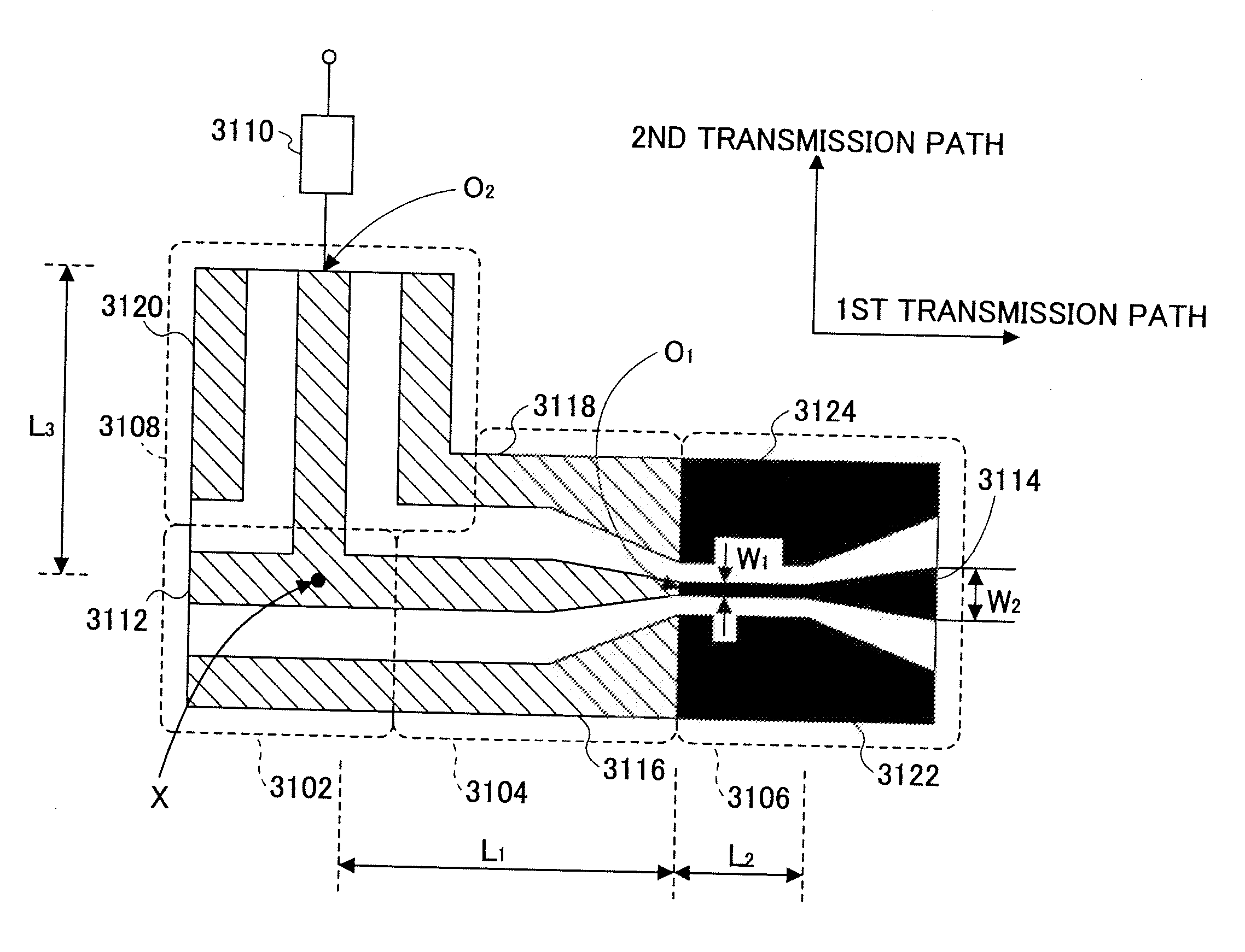
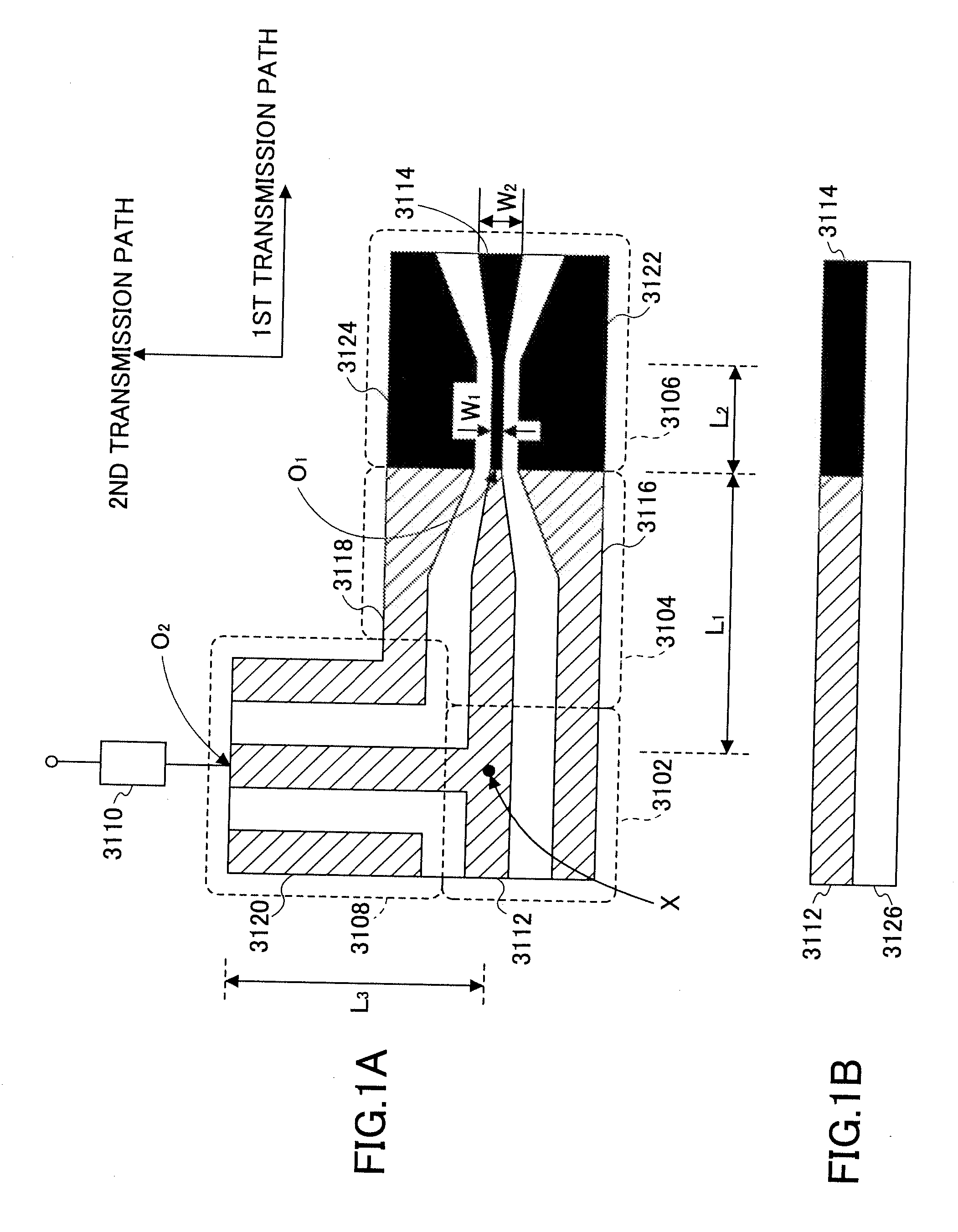
[0059]FIG. 1A is a plan view of a signal switching device 3100 as an example of a first embodiment of the present invention, and FIG. 1B is a cross-sectional side view of the signal switching device 3100 illustrated in FIG. 1A.

[0060] The signal switching device 3100 includes a switching section 3102 that switches high frequency input signals to a first transmission path or a second transmission path as described below, a first transmission section 3104 that is connected with the switching section 3102 and forms the first transmission path, a serial transmission section 3106 that is connected with the first transmission section 3104, a second transmission section 3108 that is connected with the switching section 3102 and forms the second transmission path, and a switch 3110 that is connected with the second transmission section 3108. These transmission sections are formed by a coplanar wave guide. Strip conductors 3112 and 3114 are provided at centers of the first tran...

second example

[0078]FIG. 4A is a plan view of a signal switching device 3400 as a second example of the first embodiment of the present invention, and FIG. 4B is a cross-sectional side view of the signal switching device 3400 shown in FIG. 4A.

[0079] Similar to the signal switching device 3100 described above, the signal switching device 3400 includes a switching section 3402 that switches high frequency input signals to a first transmission path or a second transmission path, a first transmission section 3404 that is connected with the switching section 3402 and forms the first transmission path, a serial transmission section 3406 that is connected with the first transmission section 3404, a second transmission section 3408 that is connected with the switching section 3402 and forms the second transmission path, and a switch 3410 that is connected with the second transmission section 3408. These transmission sections are formed by a coplanar wave guide. Strip conductors 3412 and 3414 are provide...

third example

[0092]FIG. 6A is a plan view of a signal switching device 3500 as a third example of the first embodiment of the present invention, and FIG. 6B is a cross-sectional side view of the signal switching device 3500 shown in FIG. 6A.

[0093] The signal switching device 3500 includes a switching section 3502 that switches high frequency input signals to a first transmission path or a second transmission path, a first transmission section 3504 that is connected with the switching section 3502 and forms the first transmission path, a serial transmission section 3506 that is connected with the first transmission section 3504, a second transmission section 3508 that is connected with the switching section 3502 and forms the second transmission path, and a switch 3510 that is connected with the second transmission section 3508. These transmission sections are formed by a micro-strip line. The serial transmission section 3506 is made from a superconducting material; the switching section 3502, t...


PUM


Abstract

A signal switching device including a plurality of transmission paths connected to an input path, the signal switching device outputting a signal from the input path through one of the transmission paths, including a first variable impedance unit connected to a first transmission path, the first variable impedance unit including a first section formed from a superconducting material, the first section being set to a non-superconducting state when the signal is to be output through a second transmission path, the first section including a portion of a predetermined length at an input end, the portion having an area of a cross section less than an area of a cross section of the first section at an output end.

Description

CROSS-REFERENCE TO RELATED APPLICATIONS [0001] This application is a Divisional of and claims the benefit of priority under 35 USC § 120 from U.S. Ser. No. 10 / 702,573, filed Nov. 7, 2003 based on Japanese Priority Patent Application No. 2002-324422 filed on Nov. 7, 2002, and Japanese Priority Patent Application No. 2003-015351 filed on Jan. 23, 2003, the entire contents of which are hereby incorporated by reference.BACKGROUND OF THE INVENTION [0002] 1. Field of the Invention [0003] The present invention generally relates to a high frequency circuit, in particular, to a signal switching device that switches a transmission path to which an input signal propagates. [0004] 2. Description of the Related Art [0005] In radio base stations, transponders, or other communication equipment used in cellular communications or satellite communications, signal switching devices are utilized for appropriately switching transmission paths of input signals. Such a signal switching device receives hig...

Claims


Application Information

Patent Timeline
Patent Type & Authority Applications(United States)
IPC IPC(8): H04Q11/00H01P1/10H01P1/12H01P1/15
CPCH01P1/127H01P1/15Y10S505/856Y10S505/701Y10S505/703Y10S505/866
Inventor KAWAI, KUNIHIROKOIZUMI, DAISUKESATOH, KEINARAHASHI, SHOICHIHIROTA, TETSUO
Owner NTT DOCOMO INC
Why Eureka
Try Eureka