
Method for forming thin film transistor

a thin film transistor and pattern technology, applied in the field of pattern formation, can solve the problems of poor adhesion between the film and the substrate, thermal expansion coefficient, and substrate warpage, and achieve the effect of reducing the stress of the film efficiently and improving the yield rate of the thin film transistor

Inactive Publication Date: 2007-10-11
CHUNGHWA PICTURE TUBES LTD
View PDF4 Cites 2 Cited by
  • Summary
  • Abstract
  • Description
  • Claims
  • Application Information

AI Technical Summary

Benefits of technology

[0009] A main purpose of the present invention is to provide a method for forming a pattern suitable for reducing the stress of a film and forming the pattern under the condition of a large-sized film.
[0010] A second purpose of the present invention is to provide a method for forming a thin film transistor. The method utilizes the above mentioned to reduce the stress of the film and improve the yield rate of the thin film transistor.
[0011] As embodied and broadly described herein, the present invention provides a method for forming a pattern. First, a substrate is provided. After that, a discontinuous film is formed on the substrate to reduce the stress of the film. Finally, the discontinuous film is patterned to form a pattern.
[0027] The invention utilizes the method for forming a pattern of a discontinuous film, to avoid the substrate from being warped due to the uneven stress. The invention can reduce the stress of the films efficiently under the condition of a large-sized film. Besides, the method for forming a pattern of the present invention can be applied to the fabrication process of the thin film transistor in order to improve the yield rate of the thin film transistor.

Problems solved by technology

Especially, the uneven stress would occur between different layers, which have the large difference in thermal expansion coefficient, after a high temperature process, and therefore the substrate is severely warped.
It means that the adhesion between the film and the substrate, or between different films is poor, such that the film would peel.
Besides, during the photolithography process, the misalignment and exposure shifting would occur due to the warped substrate.
However, the problem caused by the uneven stress between the films becomes more and more serious with the increased size of the film, and therefore the development of the large-sized LCD TV would be limited.

Method used


Image

  • Method for forming thin film transistor
  • Method for forming thin film transistor
  • Method for forming thin film transistor

Examples


first embodiment

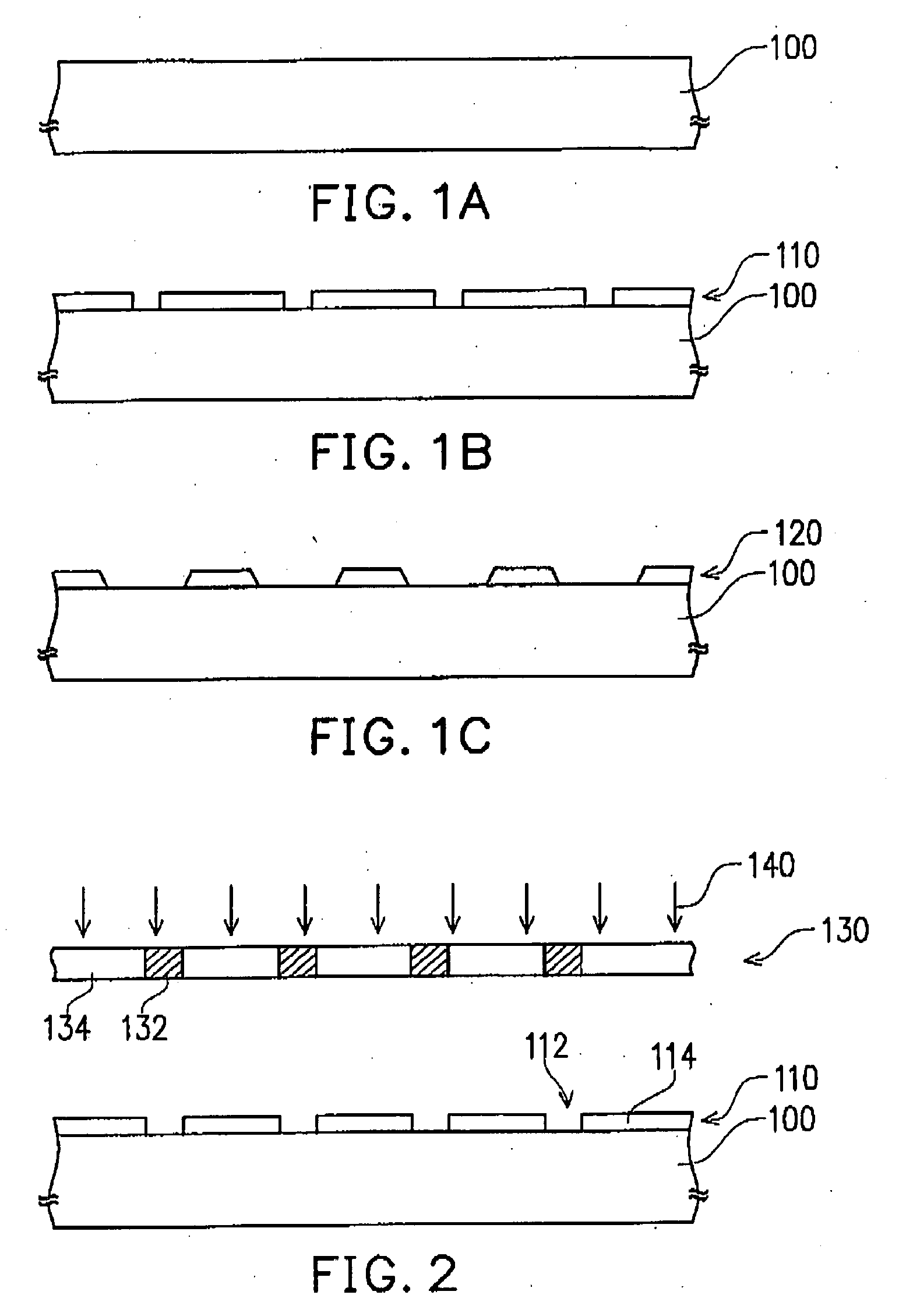
[0039]FIGS. 1A to 1C are schematic, cross-sectional diagrams illustrating the process flow for forming a pattern according to a preferred embodiment of the present invention. First, please refer to FIG. 1A, a substrate 100 is provided. Next, please refer to FIG. 1B, a discontinuous film 110 is formed on the substrate 100 to reduce the stress of the film 110. Finally, please refer to FIG. 1C, the discontinuous film 110 is patterned to form a pattern 120.

[0040] In an embodiment of the present invention, the method for forming the discontinuous film 110 on the substrate 100 as shown in FIG. 1B comprises a step of performing a deposition process 140 (shown in FIG. 2) by using a shadow mask 130. The deposition process 140 can be a chemical vapor deposition (CVD) process or a physical vapor deposition (PVD) process.

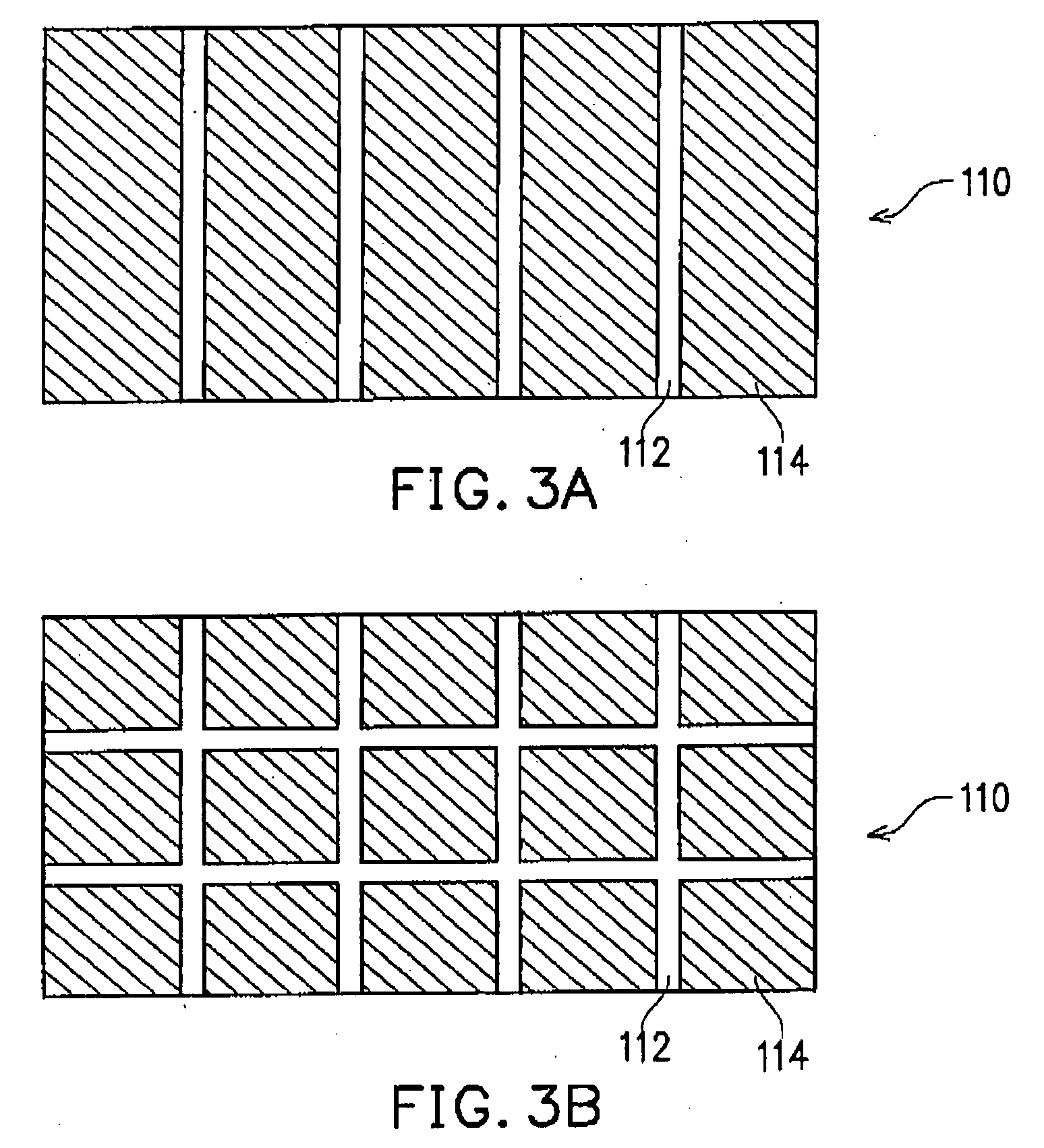
[0041]FIG. 2 is a schematic side view showing that a deposition process is performed by using a shadow mask according to a preferred embodiment of the present invention. Plea...

second embodiment

[0048] The method for forming a pattern of the first embodiment can be applied to the fabrication process of a thin film transistor of the second embodiment. The thin film transistor can be a low temperature poly silicon thin film transistor (LTPS TFT) for example. FIGS. 6A to 6G are schematic, cross-sectional diagrams illustrating the process flow for making a thin film transistor according to a preferred embodiment of the present invention.

[0049] First, please refer to FIG. 6A, a substrate 300 is provided. The substrate 300 can be a glass substrate, a silicon substrate or a flexible substrate for example.

[0050] Next, a poly silicon island 340 is formed on the substrate 300 (as shown in FIG. 6D). In an embodiment of the present invention, the method of forming the poly silicon island 340 is shown in FIGS. 6B to 6D for example. Please refer to FIG. 6B, an amorphous silicon layer 320 is formed on the substrate 300 while the amorphous silicon layer 320 is a discontinuous film. Next,...

third embodiment

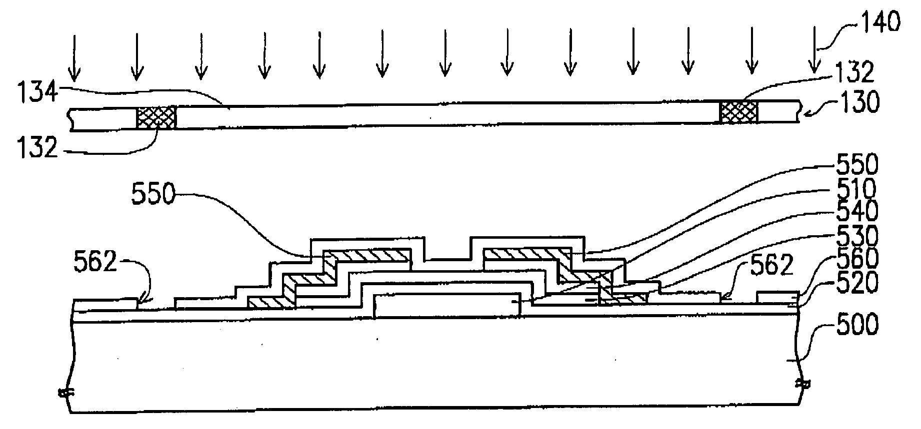
[0061]FIGS. 9A to 9E are schematic, cross-sectional diagrams illustrating the process flow for forming a thin film transistor according to another embodiment of the present invention.

[0062] First, please refer to FIG. 9A, a gate 510 is formed on a substrate 500. Next, please refer to FIG. 9B, a gate insulating layer 520 is formed on the substrate 500 to cover the gate 510. After that, please refer to FIG. 9C, a channel layer 530 is formed on the gate insulating layer 520 and the gate 510. Thereafter, please refer to FIG. 9D, a source / drain 550 is formed on the channel layer 530. At least one of the gate 510, the channel layer 530 and the source / drain 550 is formed by using the method for forming a pattern disclosed in the first embodiment.

[0063] Next, please refer to FIG. 9C, in an embodiment of the present invention, before the source / drain 550 is formed, the method further comprises a step of forming an ohmic contact layer 540 on the channel layer 530 for example. The ohmic cont...


PUM


Abstract

A method for forming a pattern is provided. First, a substrate is provided. Then, a discontinuous film is formed on the substrate so as to reduce the stress of the film. After that, the discontinuous film is patterned to form a pattern. Besides, a method for manufacturing a thin film transistor (TFT) is also provided. First, a substrate is provided. Then, a poly silicon island is formed on the substrate. After that, a gate insulating layer is formed to cover the poly silicon island. Then, a gate is formed on the gate insulating layer. After that, a source / drain is formed in the poly silicon island below one side and the other side of the gate respectively, and a channel layer is formed between the source / drain. At least one of the poly silicon island and the gate is formed according to the above mentioned method for forming the pattern.

Description

CROSS-REFERENCE TO RELATED APPLICATION [0001] This application is a divisional of a prior application Ser. No. 11 / 163,933, filed Nov. 4, 2005, now pending. The entirety of the above-mentioned patent application is hereby incorporated by reference herein and made a part of this specification.BACKGROUND OF THE INVENTION [0002] 1. Field of the Invention [0003] The present invention generally relates to a method for forming a pattern. More particularly, the present invention relates to a method for forming a pattern capable of reducing the stress of a film, and a method for forming a thin film transistor using said method. [0004] 2. Description of Related Art [0005] The display apparatus is the communication interface between user and information media. Currently, the flat panel display is the trend in development. The flat panel display mainly includes organic electro-luminescence display (OELD), plasma display panel (PDP), thin film transistor liquid-crystal display (TFT-LCD) and so o...

Claims


Application Information

Patent Timeline
Patent Type & Authority Applications(United States)
IPC IPC(8): H01L21/84
CPCH01L21/28506H01L21/31144H01L21/32051H01L29/66757H01L21/76802H01L21/76838H01L27/1214H01L21/76801H01L27/1288
Inventor CHANG, HSI-MING
Owner CHUNGHWA PICTURE TUBES LTD
Learn More