
Photonic- and phononic-structured pixel for electromagnetic radiation and detection

a phononic structure and electromagnetic radiation technology, applied in the direction of optical radiation measurement, instruments, spectrometry/spectrophotometry/monochromators, etc., can solve the problems of reducing thermal conductivity and phononic structures within nanowires, and achieve similar effectiveness, minimize electron scattering, and maximize phonon scattering/resonance

Active Publication Date: 2021-12-09
CARR WILLIAM N
View PDF0 Cites 3 Cited by
  • Summary
  • Abstract
  • Description
  • Claims
  • Application Information

AI Technical Summary

Benefits of technology

The patent describes a method of making nanowires that have reduced thermal conductivity and can also be electrically isolated. The nanowires have a sandwich structure with a layer of dielectric material between the first and second layers, which helps to reduce stress across the platform. The nanowires can also have more than three layers. These features make the nanowires better suited for use in various applications such as electronics and sensors.

Problems solved by technology

Phononic structures within the nanowires reduce the thermal conductivity.

Method used


Image

  • Photonic- and phononic-structured pixel for electromagnetic radiation and detection
  • Photonic- and phononic-structured pixel for electromagnetic radiation and detection
  • Photonic- and phononic-structured pixel for electromagnetic radiation and detection

Examples


example 1

elength Pyrometer

[0126]FIG. 9 depicts an apparatus comprised of multiple detector micro-platforms similar to the depiction of FIG. 8, physically configured to provide a standoff infrared analyzer for monitoring the temperature of thermal radiation 910 from a standoff media 920. Multiple detectors 940 are sensitive to separate wavelength bands of thermal radiation 910 emitted from standoff media 920. Optics 930 focus the radiation 910 from the remote media 920 onto the detectors 940. In this embodiment, signal conditioning circuitry 950 with an interface to a digital bus permits a determination of the temperature of a standoff media based on differential spectral analysis of the emitted thermal radiation. The pyrometer is calibrated using standoff media 920 of known temperature or known emissivity.

example 2

e Photospectrometer

[0127]FIG. 10 depicts the pixel configured to provide a reflective photospectrometer comprising both an infrared source and an infrared detector for spectral analysis of reflectance from a standoff media. This configuration permits the use of a pulsed, infrared emitter 1010 and synchronous detection with detectors 1050, 1060 thereby increasing the signal-to-noise ratio of detected infrared reflection from media 1020. The spectrometer is comprised of both an emitter 1010 which illuminates a standoff media 1020 through focusing optics 1040. Detectors depicted as 1050 and 1060 monitor different wavelengths of reflection from media 1020. Platforms comprising the emitter 1010 and detector 1050,1060 are typically comprised of MM plasmonic absorbers. The reflectance 1030 from the standoff media 1020 is determined by the surface and near surface permittivity at various depths from the surface of the standoff media 1020. The detectors 1050 and 1060 are structured to provid...

example 3

e Photospectrometer

[0128]FIG. 11 depicts the pixel adapted to provide an absorptive photospectrometer wherein synchronization for double-switched noise is provided with control and detection circuits. This type of synchronized switching is also known as correlated double-sampling (CDS) and is well known to those skilled in the art as a means for reducing noise originating between the two sampling switches. This illustrative embodiment is comprised of an infrared emitter 1120 which transmits an infrared broadband beam with collimating optics 1130 transmitting through a semi-transparent media of interest 1140. The infrared beam attenuated by media 1140 terminates into infrared detectors 1150-1154. These detectors are each sensitive to a preselected wavelength band or multiple wavelength bands. The plurality of detectors tuned to various infrared wavelengths are disposed on separate micro-platforms. Controller 1110 temperature-cycles the micro-platform in synchronization with the detec...


PUM

PropertyMeasurementUnit
thicknessaaaaaaaaaa
temperatureaaaaaaaaaa
wavelength bandaaaaaaaaaa

Abstract

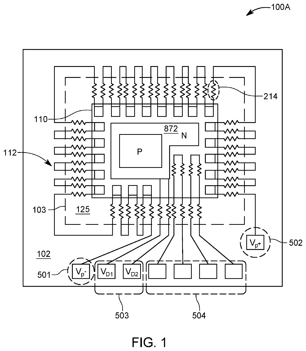
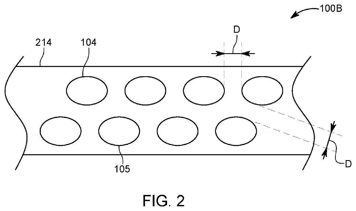
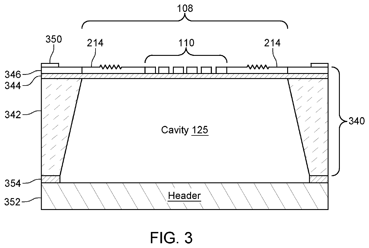
A thermal pixel configured as an electromagnetic emitter and / or an electromagnetic detector. The thermal pixel comprises a micro-platform suspended with semiconductor nanowires from a surrounding support platform. The nanowires comprise phononic structure providing a decrease in thermal conductivity. In some embodiments, the pixel is structured for operation within a broad bandwidth or a limited bandwidth. Metamaterial and / or photonic crystal filters provide pixel operation over a limited bandwidth. In some other embodiments, the micro-platform comprises a nanotube structure providing a broadband emission / absorption spectral response.

Description

STATEMENT OF RELATED CASES[0001]This case is a continuation-in-part of U.S. patent application Ser. No. 16 / 501,641 filed May 16, 2019, U.S. patent application Ser. No. 16 / 221,500 filed Dec. 15, 2018, U.S. patent application Ser. No. 15 / 805,698 filed Nov. 7, 2017, U.S. patent application Ser. No. 15 / 727,249 filed Oct. 6, 2017, U.S. patent application Ser. No. 15 / 632,462 filed Jun. 26, 2017, and U.S. patent application Ser. No. 15 / 626,151 filed Jun. 18, 2017. These applications are incorporated herein by reference. If there are any contradictions or inconsistencies in language between the present specification, and the aforementioned applications that are incorporated by reference that might affect the interpretation of the claims in this case, the claims in this case should be interpreted to be consistent with the language in this case.FIELD OF THE INVENTION[0002]The present invention pertains to an apparatus comprising a nanostructured pixel for sourcing and detection of photonic el...

Claims


Application Information

Patent Timeline
Patent Type & Authority Applications(United States)
IPC IPC(8): G01J5/12G01J5/20G01J5/06G01J5/08
CPCG01J5/12G01J5/20G01J5/061G01J2005/0077G01J5/0853G01J2005/062G01J5/0896G01J3/108G02F2202/30G02F2202/32G01J2005/202G01J2005/123G01J5/023G01J5/0225B82Y20/00G01J3/36G01J3/42G01J5/14B82Y15/00
Inventor CARR, WILLIAM N.
Owner CARR WILLIAM N
Learn More