Coatings for multilayer insulation materials

a multi-layer insulation and coating technology, applied in the field of multi-layer insulation materials, can solve the problems of low solar absorption ratio, easy damage or removal of ito coating on silver teflon, film is prone to overheating in sunlight, etc., and achieves the effect of selectively increasing or decreasing reducing and increasing the solar absorption ratio

Active Publication Date: 2020-10-27
NASA
View PDF16 Cites 2 Cited by
  • Summary
  • Abstract
  • Description
  • Claims
  • Application Information

AI Technical Summary

Benefits of technology

[0025]In some embodiments, roughening the substrate surface by texturing, etching, or adding a conductive filler increases solar absorbance without substantially changing IR emittance, while use of a smoother substrate, e.g., non-conductive polyimide, decreases solar absorbance. In other embodiments, changing the oxide thickness, e.g., alumina thickness, in the GCC coating changes IR emittance without a large impact on solar absorbance. Thus, the ratio of solar absorbance to IR emittance (a / EN) may be selectively increased or decreased by changing either or both the solar absorbance and IR emittance.
[0026]In various embodiments, the improved Goddard Composite Coating is prepared by sequential vacuum deposition of a layer of a nickel-chromium alloy; a layer of a reflective metal; a layer of aluminum oxide; a layer of silicon oxide; and optionally an ITO layer on a substrate. The substrate may have a textured surface with features having a peak height of 100 nm to 10 microns. Vacuum deposition is carried out slowly, to prevent cracking or crazing of the Goddard Composite Coating. Vacuum deposition may be electron beam physical vapor deposition, resistive thermal physical vapor deposition, or chemical vapor deposition. Vacuum deposition is carried out at 0.1 to 10 Å / sec, 0.5 to 5 Å / sec, 1 to 4.5 Å / sec, or 2 to 4 Å / sec. Vacuum deposition may be carried out on a flat film surface; on the surface of a film wrapped around the outer surface of a rotating drum; on the surface of a film wrapped around the inner surface of a hollow rotating drum; or on the surface of a film secured to a flat surface or a moving belt. In vapor deposition, the portion of the substrate closest to the deposition target may have an excessively thick coating, while the substrate edges may have a thin coating. To avoid this, a mask or deposition baffle may be placed between the deposition target and the substrate. Regions of the substrate close to the target are partially blocked, so that deposition proceeds evenly across the surface. Slow deposition as described herein leads to reduced film stress in the oxide layers, and prevents or reduces the occurrence of cracking or crazing in the GCC multilayer film. Slow deposition also reduces the incidence of delamination.
[0027]In various embodiments, the improved Goddard Composite Coating is used on a substrate for a multilayer insulation blanket in spacecraft. The improved Goddard Composite Coating, in conjunction with an appropriate substrate, may be used to set IR emittance and solar absorbance to desired values, to achieve a desired ratio of solar absorbance to IR emittance. If an ITO film is used on the Goddard Composite Coating, the ITO film allows dissipation of static charge. This prevents arcing, which potentially could damage sensitive equipment or cause radio interference.

Problems solved by technology

The polyimide substrate and aluminized films allow rapid dissipation of electrostatic charges, but do not offer a low ratio of solar absorptance (α) to IR emittance (εN).
With a high α / εN ratio, the films are prone to overheating in sunlight.
ITO-coated silver FEP Teflon does provide a low a / EN ratio, but the ITO coating on the silver Teflon is fragile easily damaged or removed.
The FEP Teflon film is susceptible to optical and structural damage in particle radiation, and is stiff and non-compliant when incorporated into a multilayer insulation (MLI) blanket.
However, Kapton® HN is a dielectric film with a smooth surface which does not allow convenient adjustment of solar absorbance.
Within limits, the α / εN ratio on such films can be altered by adjusting the thickness of the oxide layers to increase IR emittance; however, changes to the oxide layer thickness may undesirably increase IR reflectance at wavelengths above 10 microns.
Further, while increasing IR emittance lowers the α / εN ratio, IR emittance cannot be increased by adjusting oxide layer thickness above about 0.6.
Also, conventional GCC thin film coatings have a high film stress that causes the underlying polyimide film to roll tightly.
The film stress can also cause cracking or crazing during deposition of the oxide films.
In vapor deposition, the portion of the substrate closest to the deposition target may have an excessively thick coating, while the substrate edges may have a thin coating.
Increasing the thickness of the ITO film increases the conductivity of ITO, but decreases its transparency.
If sensitive electronics or electrical equipment are near the GCC film, discharge of an electrostatic charge on the film surface may cause damage to the electronics or equipment.
If no electronics or electrical equipment are near the GCC film, an ITO film may be unnecessary.
Use of a conductive, carbon filled polyimide film also causes diffuse reflection of light, while a resistive polyimide film leads to specular reflection of light.
Emittance from a Kapton® 100XC film with a GCC multilayer film on the rear surface falls outside these ranges; however, the large dip in emittance 4 inches from the film edge suggests that the Kapton® 100XC film rear surface may have an uneven oxide coating.
As shown in FIGS. 6A and 6B, an uneven oxide coating thickness can lead to changes in emittance.
In contrast, the resistive films have a smoother surface with little or no conductive carbon, leading to specular reflectance.

Method used


Image

  • Coatings for multilayer insulation materials
  • Coatings for multilayer insulation materials
  • Coatings for multilayer insulation materials

Examples


example 1

mittance of Polyimide Films with GCC Multilayer Coatings

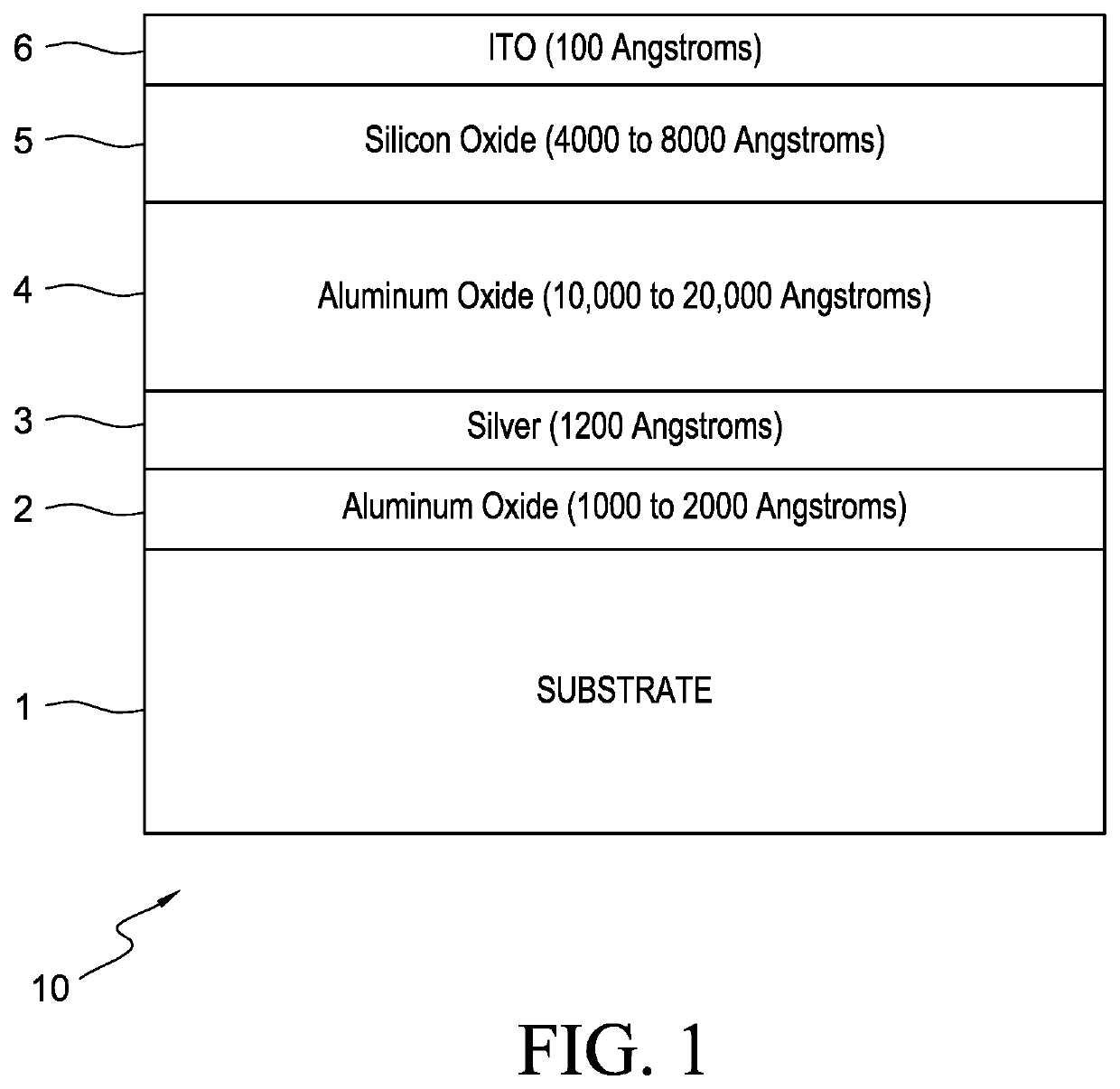
[0105]A conductive black Kapton® polyimide film was sequentially coated with a 500 angstrom layer of NiChrome alloy; a 1200 angstrom layer of silver; an ˜15,000 angstrom layer of aluminum oxide; and a ˜4,000 angstrom layer of silicon oxide. The polyimide film was 24 inches wide, and was fixed to the outer surface of a rotating drum. The various layers were evaporated from target materials in a graphite crucible using an electron beam, and deposited onto the polyimide film at a rate of between 2 and 4 angstroms per second. A central band of the film on the rotating drum was closer to the crucible than the edges of the film; a deposition baffle was used to partially protect this central band from excessive deposition and ensure an even film thickness across the width of the film. A second black polyimide film was coated in the same manner as the first film, and served as a control film.

[0106]The thicknesses of the deposited oxide...

example 2

e of Polyimide Films with GCC Multilayer Coatings

[0108]A series of black Kapton® polyimide films was obtained, as shown in Table 2 below. Two types of polyimide films were used in this example. Several films, including Kapton® 275XC, 160XC, 100XC, 200DR FC, 200DR BC, and 350DR FC, are single layer polyimide films. These films are conductive films loaded with conductive carbon. The films have black matte surfaces, and are durable from −270° C. to 270° C. Films 2 through 4 in Table 2 below are single layer polyimide films, and have front and back surfaces with similar resistivities.

[0109]Kapton®200RS100 in Table 2 below is a two layer polyimide film. On one side is a dielectric conductive film loaded with conductive carbon, while the other side is a dielectric polyimide film. The conductive surface of the film has a black matte surface, while the dielectric surface is smooth and shiny. The two layer polyimide film is durable from −270° C. to 270° C. The Kapton® XC1000, XC600, XC3500, ...

example 3

orbance / IR Emittance Ratio of Polyimide Films with GCC Multilayer Coatings

[0114]The IR emittance of the films of Table 2 was tested as a function of distance across the film, and the results for Goddard Composite coatings on both the front and back surfaces of Kapton® 200R5100, 275XC, 160XC, 100XC, XC3500, and XC300 films. As seen in FIG. 8, IR emittance one inch from the edge of the film generally ranges from 0.4 to 0.5, while IR emittance 5 inches from the edge of the film ranges from 0.54 to 0.58. Emittance from a Kapton® 100XC film with a GCC multilayer film on the rear surface falls outside these ranges; however, the large dip in emittance 4 inches from the film edge suggests that the Kapton® 100XC film rear surface may have an uneven oxide coating. As shown in FIGS. 6A and 6B, an uneven oxide coating thickness can lead to changes in emittance.

[0115]Table 3 reports values for solar absorbance and IR emittance of GCC-coated polyimide films, as well as resistance of polyimide fil...


PUM

PropertyMeasurementUnit
thickaaaaaaaaaa
thickaaaaaaaaaa
reflectanceaaaaaaaaaa

Abstract

A laminate has a composite coating on a substrate. The substrate is a polymeric substrate with a surface resistivity of 4×10² to 1×10⁸Ω/□; or a textured substrate with surface features which are 100 nm to 10 microns high. The composite coating comprising a tie layer of a nickel-chromium alloy; a layer of a reflective metal; a layer of aluminum oxide; a layer of silicon oxide; and optionally a layer of indium tin oxide. The laminate has a solar absorbance at a wavelength of 0.25 microns to 2.5 microns of between 0.07 and 0.7; and the laminate has an IR emittance of 0.1 to 0.8. Solar absorbance and IR emittance of the laminate may be independently to control the ratio of solar absorbance to IR emittance. Solar absorbance may be adjusted by changing the surface resistance or degree of texturing on the substrate. IR emittance may be adjusted by changing oxide film thickness.

Description

ORIGIN OF THE INVENTION[0001]The invention described herein was made by an employee of the United States Government, and may be manufactured and used by or for the Government for Government purposes without the payment of any royalties thereon or therefore.TECHNICAL FIELD[0002]This disclosure relates generally to multilayer insulation materials for use in space environments, which offer low solar absorbance, low IR reflectance, and high IR emittance. The materials can be made to reduce specularity and provide charge bleed off characteristics.BACKGROUND[0003]In charging environments such as geosynchronous orbit, commonly used include coated or uncoated black polyimide films, such as black Kapton®, Germanium coated black Kapton® or StaMet™ coated black Kapton®, aluminized films, or Indium tin oxide (ITO) coated silver FEP Teflon, where FEP Teflon is poly(tetrafluoroethylene-co-hexafluoropropylene). The polyimide substrate and aluminized films allow rapid dissipation of electrostatic c...

Claims


Application Information

Patent Timeline
Patent Type & Authority Patents(United States)
IPC IPC(8): B32B15/04B32B17/06B64G1/22C23C14/08C23C14/20C23C14/10C23C14/30
CPCC23C14/10C23C14/081C23C14/086B64G1/226C23C14/20C23C14/30B64G1/50
Inventor HASEGAWA, MARK MO'CONNOR, KENNETHWONG, ALFREDHARRIS, GEORGE M.SMITH, GRANT
Owner NASA
Why Eureka
Try Eureka