Annealing method and annealing apparatus

a technology of annealing method and annealing apparatus, which is applied in the direction of laser beam welding apparatus, manufacturing tools, welding/soldering/cutting articles, etc., can solve the problems of affecting the annealing efficiency of laser beam, and affecting the annealing process. stable, the effect of improving the annealing efficiency

Inactive Publication Date: 2012-09-06
TOKYO ELECTRON LTD
View PDF11 Cites 13 Cited by
  • Summary
  • Abstract
  • Description
  • Claims
  • Application Information

AI Technical Summary

Benefits of technology

[0010]According to the present invention, since the laser beam is incident obliquely on the surface of the target object, the laser absorption efficiency can be s...

Problems solved by technology

When the laser beam is irradiated in the above manner, there is a possibility that the laser beam might not be efficiently absorbed by a film formed on the surface of the semiconductor wafer, since the film thickness is small with respect to the wavelength of the far infrared laser beam.
If the laser beam transmits through the film and the wafer to a certain degree, the reflected light on the front sur...

Method used


Image

  • Annealing method and annealing apparatus
  • Annealing method and annealing apparatus
  • Annealing method and annealing apparatus

Examples


first embodiment

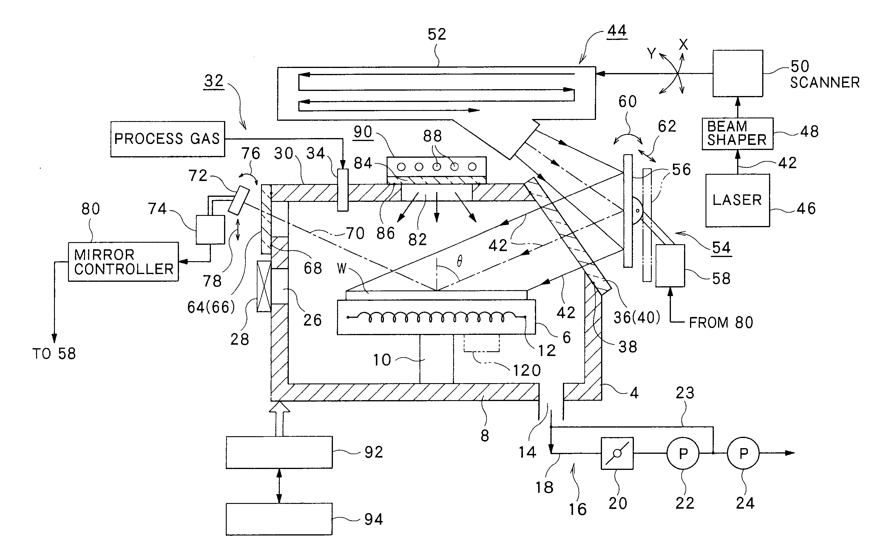
[0017]FIG. 1 is a configuration diagram showing a first embodiment of an annealing apparatus according to the present invention. As shown in FIG. 1, the annealing apparatus 2 includes a processing vessel 4 capable of accommodating therein a target object, such as a semiconductor wafer W. The processing vessel 4 has a box-like shape made of, e.g., aluminum, an aluminum alloy or a stainless steel.

[0018]Inside the processing vessel 4, a stage 6 configured to hold the wafer W is disposed. The stage 6 is supported by a column 10 standing from a bottom part 8 of the processing vessel 4. The wafer W can be placed on an upper surface of the stage 6. For example, a wafer having a diameter of 300 mm is used as the wafer W. The stage 6 is made of, e.g., aluminum, an aluminum alloy or a ceramic. A heater 12 for heating the wafer W is disposed inside the stage 6, so that the wafer W can be heated according to need. There is a case in which the heater 12 is not provided. The stage 6 is provided w...

second embodiment

[0056]Next, a second embodiment of the annealing apparatus is described below. FIG. 4 is a schematic configuration diagram showing the second embodiment of the annealing apparatus of the present invention. FIG. 4 shows in detail a main part of the annealing apparatus in the second embodiment (part different from the first embodiment), while the other parts are omitted or simplified. In FIG. 4, the same constituent elements as those shown in FIG. 1 are designated by the same reference numbers, and duplicated description thereof is omitted.

[0057]In the first embodiment shown in FIG. 1, the multipath unit 52 is arranged above the processing vessel 4. On the other hand, as shown in FIG. 4, in the annealing apparatus 2 in the second embodiment, the multipath unit 52 is arranged to stand on a lateral side of the processing vessel 4. Also in this embodiment, the reflection mirror 56 of the incident angle adjusting mirror unit 54 can be moved in an optical axis direction as shown by an arro...


PUM

PropertyMeasurementUnit
Angleaaaaaaaaaa
Angleaaaaaaaaaa
Wavelengthaaaaaaaaaa

Abstract

An annealing method irradiates a target object, having a film formed on its surface, with a laser beam to perform an annealing process to the target object. The surface of the target object is irradiated with the laser beam obliquely at an incident angle that is determined to achieve an improved laser absorptance of the film.

Description

CROSS REFERENCE TO RELATED APPLICATION[0001]The present application is based on and claims the benefit of priority from U.S. provisional application No. 61 / 448,848 filed on Mar. 3, 2011, the entire contents of which are incorporated herein by reference.TECHNICAL FIELD[0002]The present invention relates to a method and apparatus for annealing a film formed on a surface of a target object, such as a semiconductor wafer.BACKGROUND ART[0003]In general, in order to manufacture a semiconductor device or the like, various processes, such as a film deposition process, an etching process, an oxidation process, an annealing process and a modification process, are repeatedly performed to a semiconductor wafer such as a silicon substrate. Among these processes, the annealing process heats a semiconductor wafer to a predetermined temperature, in order to improve properties of a film formed on a surface of the semiconductor wafer. Recently, in order to expedite the annealing process and in order ...

Claims


Application Information

Patent Timeline
IPC IPC(8): H01L21/26B23K26/42B23K26/12B23K26/08
CPCB23K26/0081B23K26/0807B23K26/122B23K26/127H01L21/02126H01L21/02164H01L21/324H01L21/02354H01L21/67115H01L21/268B23K26/0042B23K26/0045C03C23/0025H01L21/02337B23K26/0006B23K26/1224B23K26/082B23K2103/52B23K2103/56B23K26/354H01L21/31
Inventor IZAWA, YUSAKULIU, JUNJUNYUE, HONGYUTOMA, DOREL
Owner TOKYO ELECTRON LTD
Why Eureka
Try Eureka