CVD thin film stress control method for display application

a thin film and control method technology, applied in the direction of solid-state devices, semiconductor devices, organic semiconductor devices, etc., can solve the problems of increased drive voltage, limited lifetime of oled devices, and decreased electroluminescence efficiency

Active Publication Date: 2018-11-15
APPLIED MATERIALS INC
View PDF6 Cites 3 Cited by
  • Summary
  • Abstract
  • Description
  • Claims
  • Application Information

AI Technical Summary

Problems solved by technology

OLED devices may have limited lifetimes, characterized by a decrease in electroluminescence efficiency and an increase in drive voltage thereof.
One known reason for these degradations of OLED device performance is the formation of non-emissive dark spots or regions within an OLED display due to moisture or oxygen ingress into the organic layers of the OLED device.
It has been observed that existing encapsulation layers may have difficulty in preventing failure of OLED devices as a result of moisture or oxygen ingress into the organic layers of the OLED device over time.

Method used


Image

  • CVD thin film stress control method for display application
  • CVD thin film stress control method for display application
  • CVD thin film stress control method for display application

Examples


Embodiment Construction

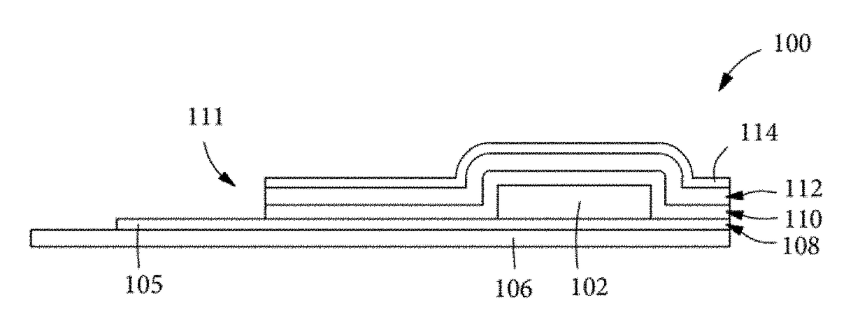
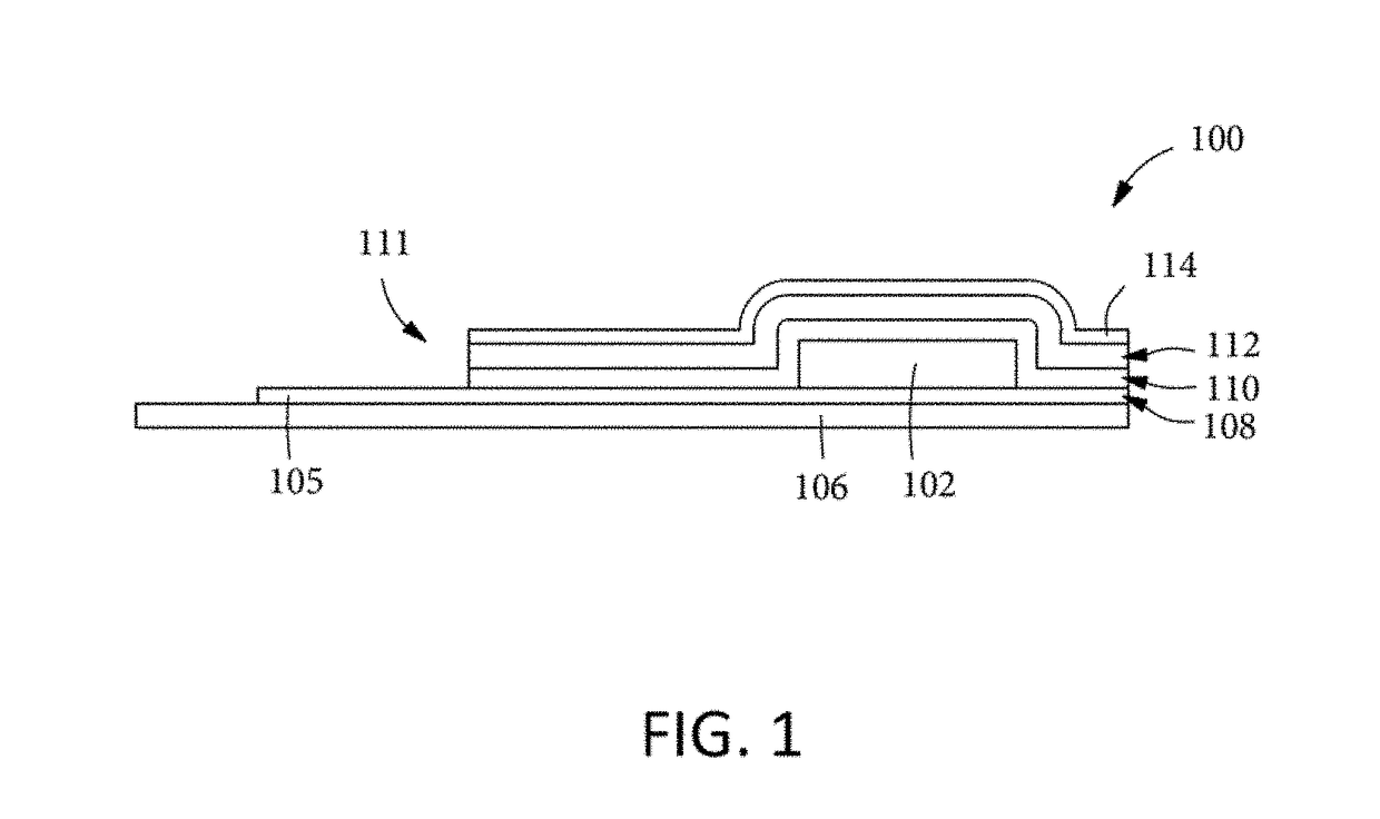
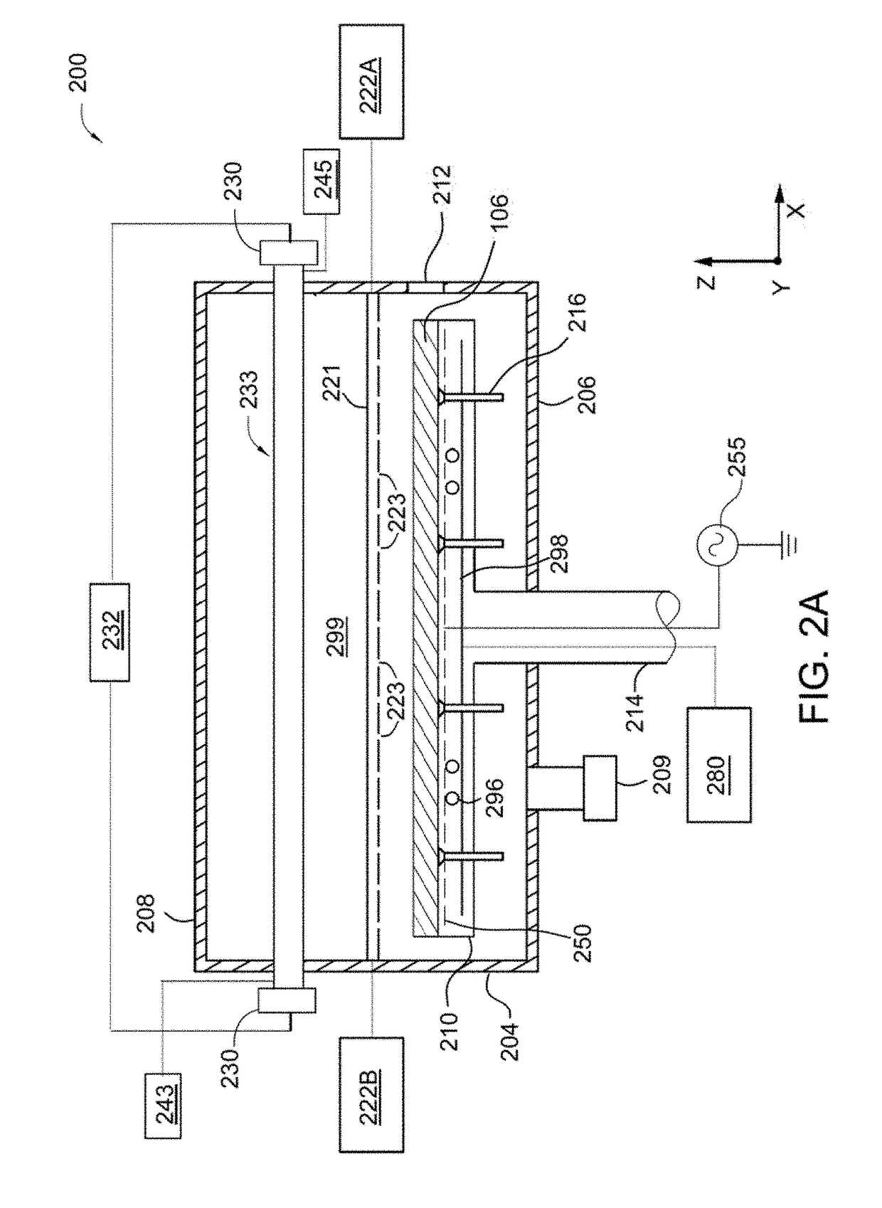
[0016]Embodiments of the present disclosure generally describe a method for depositing a barrier layer of silicon nitride on a substrate, including over previously formed layers on the substrate, using a high density plasma chemical vapor deposition (HDP-CVD) process, and in particular, controlling a film stress of the deposited silicon nitride layer by a controlled biasing of the substrate during the deposition process.

[0017]Encapsulation of OLED devices improves the lifetime of the device by preventing the degradation of the OLED device due to moisture or oxygen ingress there into. One method of forming a thin film encapsulation structure includes depositing multilayer stacks of barrier layers with buffer layers sandwiched there between. Typically the barrier layers comprise a dielectric such as silicon nitride and the buffer layers comprise a polymerized organic.

[0018]Encapsulation stacks of silicon nitride and polymerized organic film layers, using silicon nitride layers deposit...


PUM

PropertyMeasurementUnit
temperatureaaaaaaaaaa
frequencyaaaaaaaaaa
chamber pressureaaaaaaaaaa

Abstract

Embodiments of the present disclosure generally describe a method for depositing a barrier layer of SiN using a high density plasma chemical vapor deposition (HDP-CVD) process, and in particular, controlling a film stress of the deposited SiN layer by biasing the substrate during the deposition process.

Description

CROSS-REFERENCE TO RELATED APPLICATIONS[0001]This application claims benefit of U.S. Provisional Patent Application Ser. No. 62 / 506,234, filed May 15, 2017, which is herein incorporated by reference.BACKGROUNDField[0002]Embodiments described herein generally relate to a method for manufacturing a thin film encapsulation (TFE) structure for an organic light emitting diode (OLED) device and a method for depositing a silicon nitride film using high density plasma chemical vapor deposition (HDP-CVD).Description of the Related Art[0003]Organic light emitting diode displays (OLED displays) have recently gained significant interest in display applications in view of their faster response times, larger viewing angles, higher contrast, lighter weight, lower power consumption and amenability to being formed on flexible substrates as compared to conventional LCD or plasma displays. Generally, a conventional OLED device is enabled by using at least two layers of organic materials sandwiched bet...

Claims


Application Information

Patent Timeline
Patent Type & Authority Applications(United States)
IPC IPC(8): H01L51/56H01L51/52H01L51/00
CPCH01L51/56H01L51/5253H01L51/0097H01L2251/303H01L51/0035H01L2251/5338H01L2251/301H01L51/5203H10K77/111H10K50/844H10K2102/311H01L21/02274H01L21/0262H01L21/324H01L21/02208H10K71/10H10K71/00H10K50/805H10K85/111H10K2102/00
Inventor WON, TAE KYUNGCHOI, SOO YOUNGYADAV, SANJAY D.SORENSEN, CARL A.KAO, CHIEN-TEHANWAR, SUHAILLEE, YOUNG DONG
Owner APPLIED MATERIALS INC
Why Eureka
Try Eureka