Light-emitting device and manufacturing method thereof

a technology of light-emitting devices and manufacturing methods, which is applied in the direction of semiconductor devices, basic electric elements, electrical apparatus, etc., can solve the problems of low light-emitting efficiency, low light-emitting efficiency, and low light-emitting efficiency, and achieve high-efficiency light-emitting effects

Inactive Publication Date: 2007-11-01
SUMITOMO ELECTRIC IND LTD +1
View PDF17 Cites 2 Cited by
  • Summary
  • Abstract
  • Description
  • Claims
  • Application Information

AI Technical Summary

Benefits of technology

[0009] An object of the present invention is to provide a light-emitting device enabling highly efficient light emission and high-power light emission and a manufacturing method thereof.
[0011] According to the above-described construction, as the nitride semiconductor substrate having a low dislocation density is used, a density of threading dislocations operating as non-radiative centers in the light-emitting device can be decreased to increase light emission efficiency. In addition, the light emission efficiency can further be increased with a composition modulation effect by In included in the InAlGaN quaternary alloy. It is to be noted that, the nitride semiconductor substrate has conductivity of a first conductivity type, and can be any nitride semiconductor such as a GaN substrate, an AlxGa1-xN substrate (0<x<1), or an AlN substrate included in the AlxGa1-xN substrate.
[0013] The nitride semiconductor layer having thickness of at most 100 μm is formed by etching or abrasion of the aforementioned nitride semiconductor substrate in the present invention. With this construction, absorption by the nitride semiconductor substrate can be inhibited in addition to decreasing the density of threading dislocations operating as non-radiative centers and obtaining the composition modulation effect by In included in the InAlGaN quaternary alloy.
[0015] As GaN, for example, absorbs ultraviolet light having a wavelength of 360 nm or shorter, a light output can be increased by the removing or abrasion of the GaN substrate according to the above-described method. As a result, the light output can further be increased. Other nitride semiconductor may also absorb light of a wavelength region which is desired to be taken out, and in such situation, the light output can be increased by removing the nitride semiconductor substrate.

Problems solved by technology

The above-described ultraviolet light-emitting device, however, has low light emission efficiency, and the light emission efficiency decreases because of heat production when a large current is passed for use in illumination.
In particular, when a sapphire substrate is used, it does not dissipate heat efficiently and there is a strong tendency of light emission efficiency not to increase linearly in proportion to an input, but to be saturated halfway.

Method used


Image

  • Light-emitting device and manufacturing method thereof
  • Light-emitting device and manufacturing method thereof
  • Light-emitting device and manufacturing method thereof

Examples


first embodiment

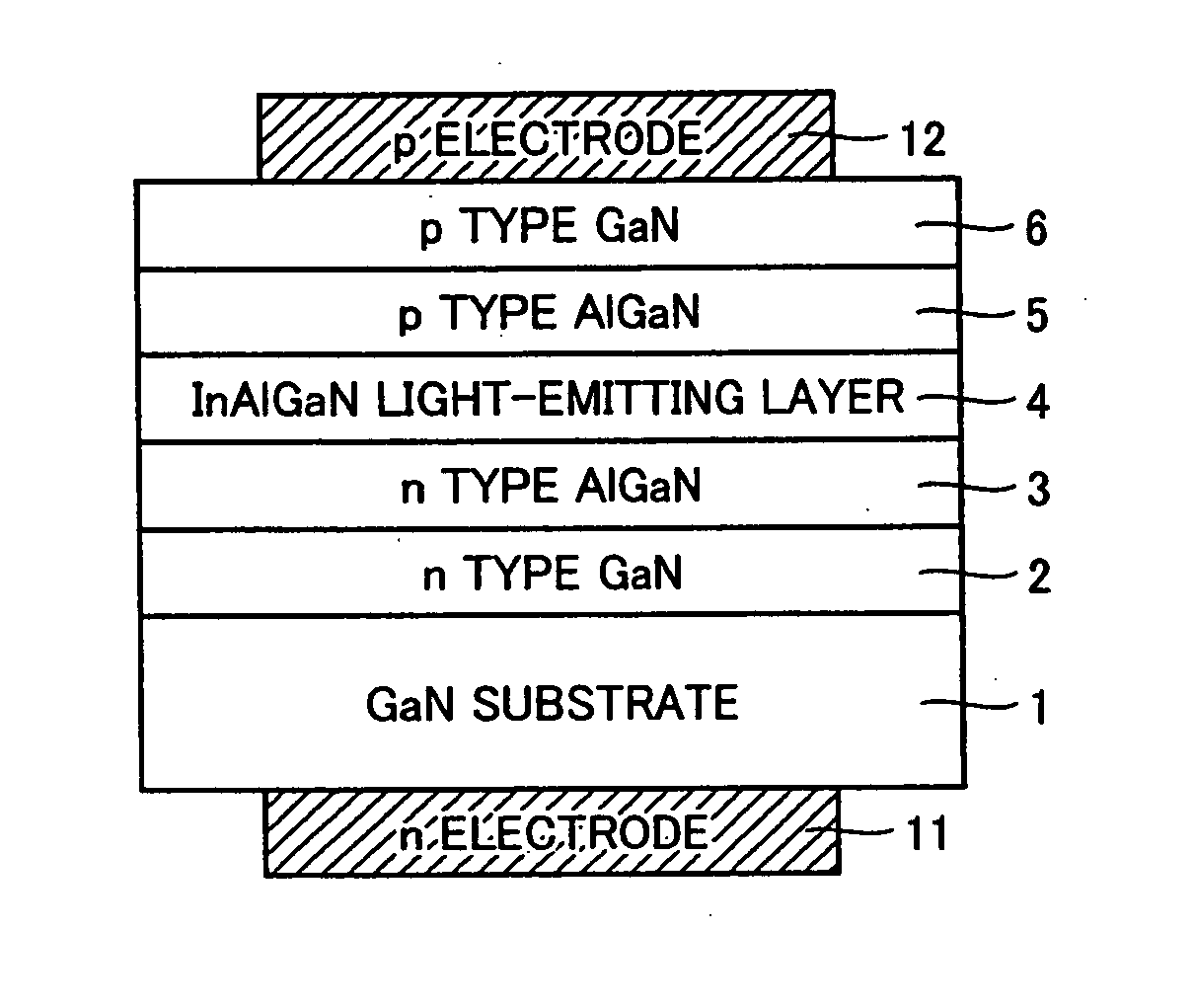
[0028]FIG. 1 shows an LED according to a first embodiment of the present invention. In FIG. 1, a stacked structure (an n type GaN layer 2 / an n type AlxGa1-xN layer 3 / an InAlGaN light-emitting layer 4 / a p type AlxGa1-xN layer 5 / a p type GaN layer 6) is formed on a GaN substrate 1. An n electrode 11 is arranged on a second main plane, that is, a backside of GaN substrate 1, while a p electrode 12 is arranged on p type GaN layer 6. Ultraviolet light is emitted from the InAlGaN light-emitting layer by applying a current to the pair of n electrode 11 and p electrode 12. The InAlGaN light-emitting layer has a composition of InxaAlyaGa1-xa-yaN.

[0029] The GaN-based I-ED shown in FIG. 1 is manufactured by the following processing steps. A GaN substrate having thickness of 400 μm, a dislocation density of 5E6 cm−2 and a resistivity of 1E-2 Ωcm was arranged on a susceptor within an MOCVD (Metal Organic Chemical Vapor Deposition) device. While the inside of the deposition reactor was kept deco...

second embodiment

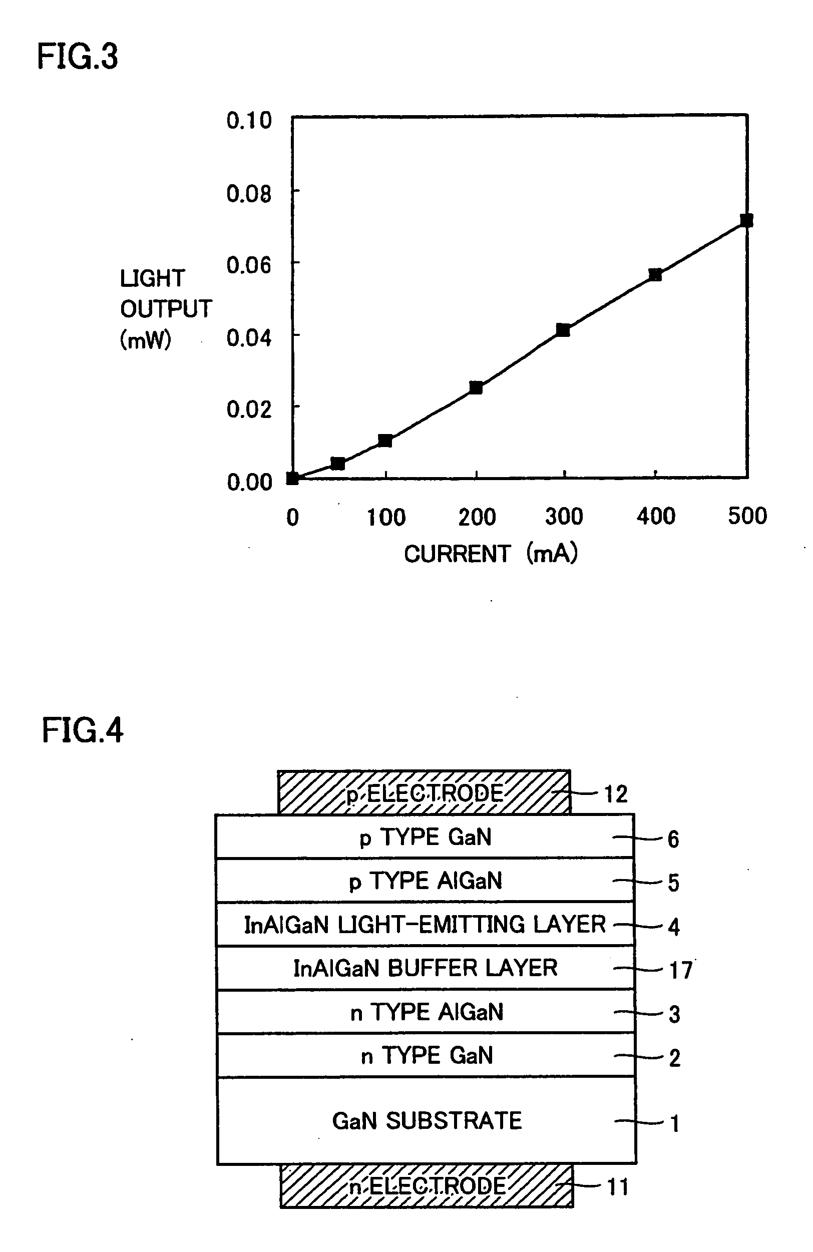
[0034]FIG. 4 shows an ultraviolet light-emitting diode according to a second embodiment of the present invention. As compared with the stacked structure of the ultraviolet LED shown in FIG. 1, this ultraviolet light-emitting diode is characterized in that, an InxAlyGa1-x-yN layer 17 as a buffer layer is arranged in contact with light-emitting layer 4 on a side nearer to GaN substrate 1. In addition, the light-emitting layer has a multiple quantum well structure, which will be described below.

[0035] A manufacturing method of the ultraviolet LED according to this embodiment is as follows. A substrate having thickness of 400 μm and a threading dislocation density of 5E6 / cm2 was used as GaN substrate 1. N type GaN layer 2 and n type AlxGa1-xN layer 3 were successively formed on GaN substrate 1 by a method similar to that in the first embodiment. Then, InxAlyGa1-x-yN buffer layer 17 having thickness of 50 nm was grown at a growth temperature of 830° C. in contact with n type AlxGa1-xN l...

third embodiment

[0041] In a third embodiment of the present invention, light outputs were compared between an ultraviolet LED formed on the GaN substrate (an example of the present invention) and an ultraviolet LED formed on a GaN template (a substrate formed by growing an n type GaN for 3 μm on a sapphire substrate via a GaN buffer layer grown at low temperature) (an comparative example). The GaN template used was made previously. Both of the aforementioned example of the present invention and comparative example were formed to have stacked structures as shown in FIGS. 4 and 5 except that, as a backside of the GaN template is an insulator, the n electrode for the GaN template was formed on the previously exposed n type GaN layer.

[0042] For manufacturing, both GaN substrate and GaN template were arranged together on the susceptor within the MOCVD device. Then, the n type GaN layer, n type Alx1Ga1-x1N layer and InxAlyGa1-x-yN layer as a buffer layer were formed on each of the GaN substrate and GaN ...


PUM

PropertyMeasurementUnit
dislocation densityaaaaaaaaaa
thicknessaaaaaaaaaa
wavelength rangeaaaaaaaaaa

Abstract

To provide a light-emitting device using a nitride semiconductor which can attain high-power light emission by highly efficient light emission and a manufacturing method thereof, the light-emitting device includes a GaN substrate and a light-emitting layer including an InAlGaN quaternary alloy on a side of a first main surface of GaN substrate.

Description

CROSS-REFERENCE TO RELATED APPLICATION [0001] This application is a Continuation of U.S. application Ser. No. 10 / 916,802 filed Aug. 11, 2004, the entirety of which is incorporated herein by reference.BACKGROUND OF THE INVENTION [0002] 1. Field of the Invention [0003] The present invention relates to a lighting device and a manufacturing method thereof More specifically, the present invention relates to a light-emitting device using a nitride semiconductor emitting ultraviolet light and a manufacturing method thereof [0004] 2. Description of the Background Art [0005] A GaN-based compound semiconductor functions as a blue TED (Light Emitting Diode) or an ultraviolet LED because of its large band gap, and is often used as an excitation light source of a white LED. Suggestions such as the following have been made for improvement of performance of the GaN-based LED which emits ultraviolet light having a short wavelength. [0006] (d1) Using a SiC substrate and an InAlGaN layer as a light-e...

Claims


Application Information

Patent Timeline
Patent Type & Authority Applications(United States)
IPC IPC(8): H01L29/22H01L33/06H01L33/12H01L33/32H01L33/36
CPCH01L33/0075H01L33/32H01L33/06H01L33/0079H01L33/0093Y02E10/548
Inventor HIRAYAMA, HIDEKIAKITA, KATSUSHINAKAMURA, TAKAO
Owner SUMITOMO ELECTRIC IND LTD
Why Eureka
Try Eureka