Light-emitting device, light-receiving device and method of manufacturing the same

a light-emitting device and light-emitting device technology, applied in the direction of lasers, semiconductor devices, semiconductor lasers, etc., can solve the problems of difficult to efficiently cause the light to be emitted, the law of momentum conservation and the law of energy conservation cannot be satisfied simultaneously, and achieves a high degree of reliability, prevent the attenuation of light, and easy formation

Inactive Publication Date: 2014-03-25
HITACHI LTD
View PDF17 Cites 3 Cited by
  • Summary
  • Abstract
  • Description
  • Claims
  • Application Information

AI Technical Summary

Benefits of technology

[0035]The effects obtained by typical embodiments of the invention disclosed in the present application will be briefly described below.
[0036]According to the present invention, a germanium laser diode and a germanium photodiode which can be easily formed by using a silicon process whose infrastructure is well-organized can be provided on an SOI substrate inexpensively and with a high degree of reliability.
[0037]According to the present invention, by applying tensile strain without using a quantum confinement effect, highly-efficient light emission from a germanium light-emitting device can be achieved. Also, by applying tensile strain, the technology of transfiguring germanium to a direct transition structure and the light confinement to prevent attenuation of light due to the electrode can be both achieved. Also, in the germanium laser diode according to the present invention, by fabricating an electrode of high-concentration silicon-germanium, the concentration of carriers of single-crystal germanium serving as a light-emitting layer can be incr...

Problems solved by technology

The light confined in the semiconductor resonator in this manner efficiently induces recoupling between the electron and the hole forming a population inversion, which thus leads to laser oscillation.
However, since silicon and germanium in a bulk state are indirect transition semiconductors, it is difficult to cause them to emit light efficiently.
Therefore, in silicon and germanium in a bulk state, in the course where an electron and a hole simply c...

Method used


Image

  • Light-emitting device, light-receiving device and method of manufacturing the same
  • Light-emitting device, light-receiving device and method of manufacturing the same
  • Light-emitting device, light-receiving device and method of manufacturing the same

Examples


first embodiment

[0156

[0157]In the present embodiment, a germanium laser diode created by a method easily achieved by a normal silicon process and a method of manufacturing the germanium laser diode will be disclosed.

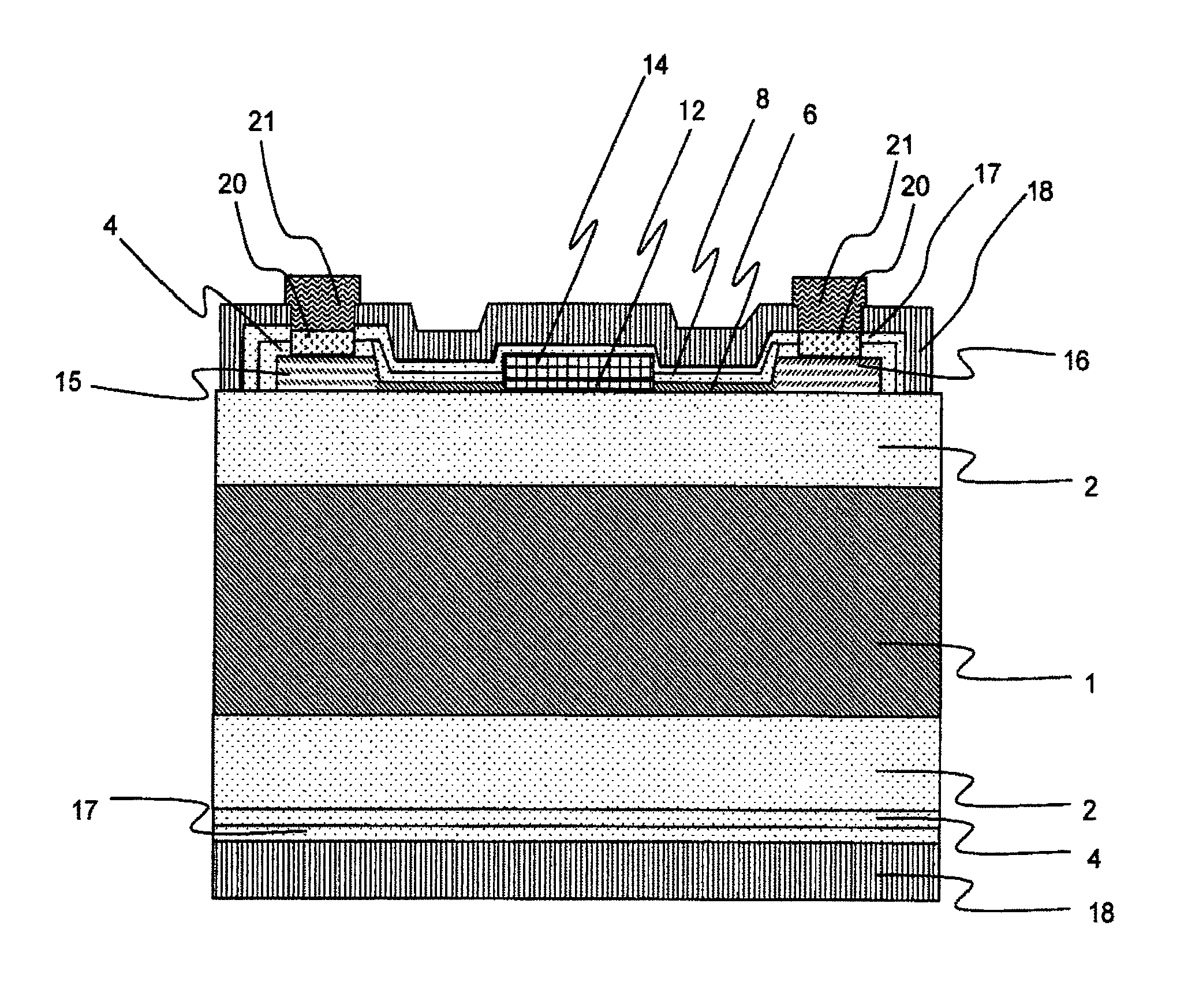
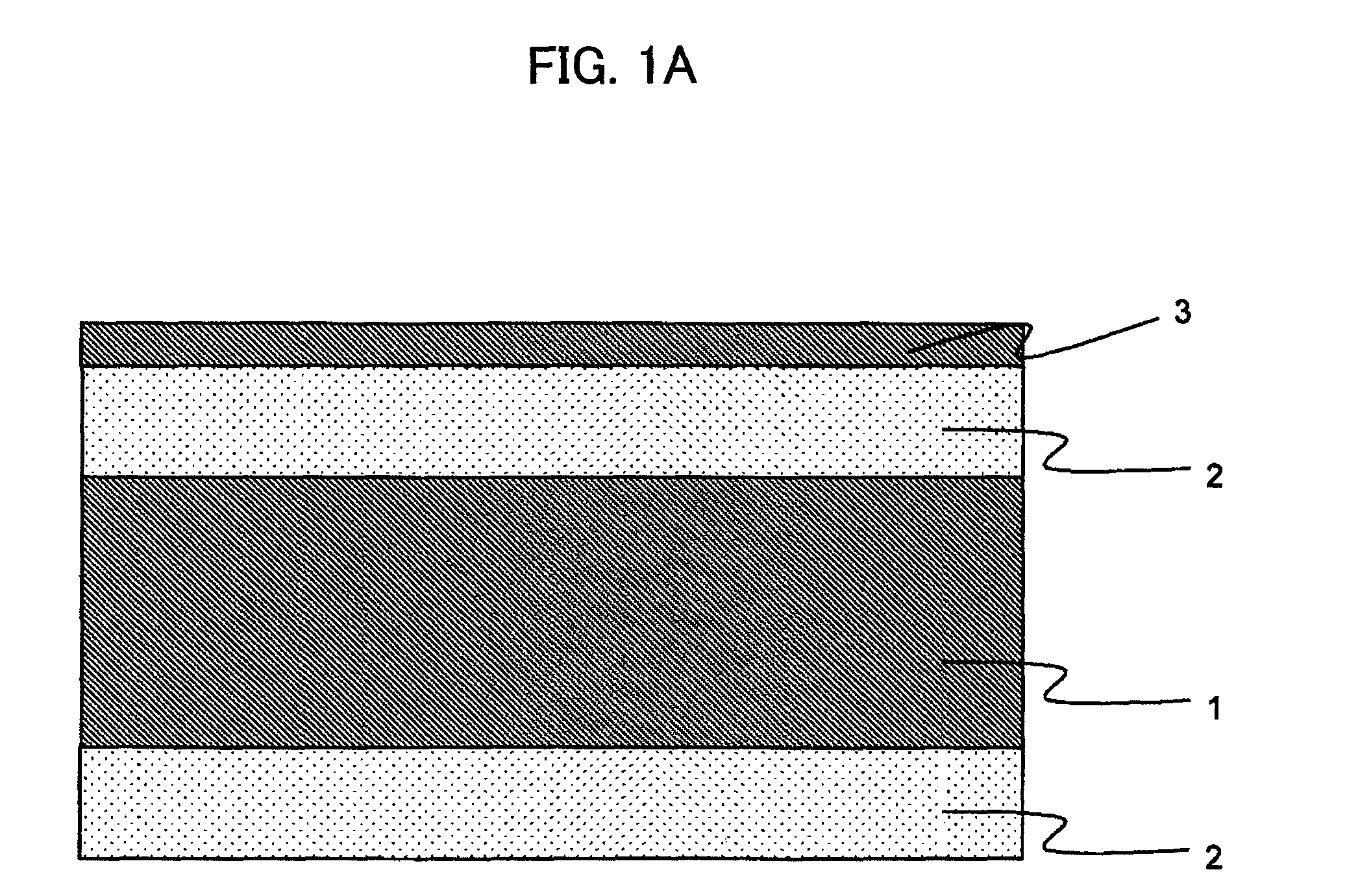
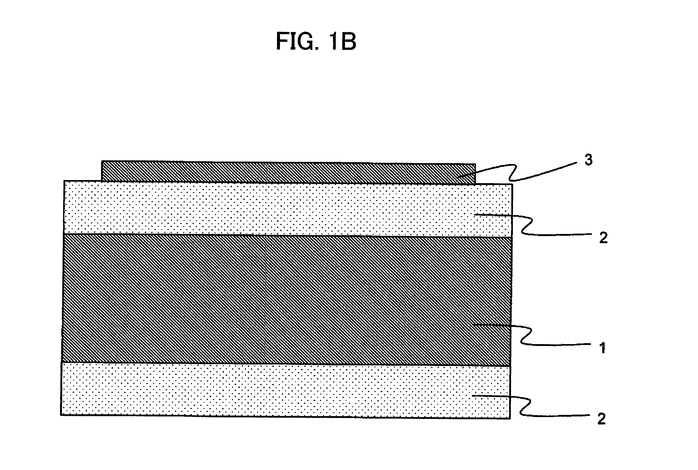
[0158]FIG. 1A to FIG. 1R each depicts a sectional structure in the order of a manufacturing process. Also, FIG. 2A to FIG. 2R depict schematic drawings viewed from above a substrate in the order of a manufacturing process. Here, FIG. 1A to FIG. 1R are sectional views in a lateral direction of FIG. 2A to FIG. 2R, respectively. For example, FIG. 1R depicts a sectional structure taken along a cutting-plane line 23 in FIG. 2R. Furthermore, FIG. 3A to FIG. 3R each depicts a sectional structure taken along a cutting-plane line 24 in FIG. 2R. The cutting-plane lines 23 and 24 are orthogonal to each other in the same plane, the cutting-plane line 23 extends in an X direction in the drawing, and the cutting-plane line 24 extends in a Y direction in the drawing. The drawings of a completed device...

second embodiment

[0195

[0196]In the present embodiment, a germanium laser diode using a distributed feed-back (abbreviated as DFB) type as a resonance structure and a method of manufacturing the germanium laser diode will be disclosed.

[0197]FIG. 4A to FIG. 4I each depicts a sectional structure in the order of a manufacturing process. Also, FIG. 5A to FIG. 5I depict schematic drawings viewed from above a substrate in the order of a manufacturing process. Here, FIG. 4A to FIG. 4I are sectional views in a lateral direction of FIG. 5A to FIG. 5I, respectively. For example, FIG. 4I depicts a sectional structure taken along a cutting-plane line 23 in FIG. 5I. Furthermore, FIG. 6I depicts a sectional structure taken along a cutting-plane line 24 in FIG. 5I. The cutting-plane lines 23 and 24 are orthogonal to each other in the same plane, the cutting-plane line 23 extends in an X direction in the drawing, and the cutting-plane line 24 extends in a Y direction in the drawing. The drawings of a completed devic...

third embodiment

[0217

[0218]In the present embodiment, a DBR germanium laser diode using STI (Shallow Trench Isolation) as a strain-applying method and a method of manufacturing the germanium laser diode will be disclosed.

[0219]FIG. 7A to FIG. 7K each depicts a sectional structure in the order of a manufacturing process. Also, FIG. 8K depicts a drawing of a completed device viewed from above the substrate. Here, FIG. 7A to FIG. 7K each depicts a structure taken along a cutting-plane line 23 in FIG. 8K. Furthermore, FIG. 9K depicts a sectional structure taken along a cutting-plane line 24 in FIG. 8K. The cutting-plane lines 23 and 24 are orthogonal to each other in the same plane, the cutting-plane line 23 extends in an X direction in the drawing, and the cutting-plane line 24 extends in a Y direction in the drawing. The drawings of a completed device in the present embodiment are FIG. 7K, FIG. 8K and FIG. 9K.

[0220]The manufacturing process will be sequentially described below. First, as depicted in ...


PUM


Abstract

An object of the present invention is to provide a germanium laser diode that can be easily formed on a substrate such as silicon by using a normal silicon process and can emit light efficiently. A germanium light-emitting device according to the present invention is a germanium laser diode characterized in that tensile strain is applied to single-crystal germanium serving as a light-emitting layer to be of a direct transition type, a thin semiconductor layer made of silicon, germanium or silicon-germanium is connected adjacently to both ends of the germanium light-emitting layer, the thin semiconductor layer has a certain degree of thickness capable of preventing the occurrence of quantum confinement effect, another end of the thin semiconductor layer is connected to a thick electrode doped with impurities at a high concentration, the electrode is doped to a p type and an n type, a waveguide is formed so as not to be in direct contact with the electrode, and a mirror is formed at an end of the waveguide.

Description

TECHNICAL FIELD[0001]The present invention relates to a light-emitting device, a light-receiving device and a method of manufacturing these devices, and more particularly to a germanium laser diode, a germanium photodiode and a method of manufacturing these diodes using tensile strain.BACKGROUND ART[0002]In a broad band network that supports the Internet industry, optical communications have been adopted. For the transmission and reception of light in the optical communications, a laser diode using a compound semiconductor of a III-V group, a II-VI group or the like has been used.[0003]Among various structures proposed for a compound semiconductor laser, a double hetero structure is a common example. In the double hetero structure, compound semiconductors of two different types are used, and a compound semiconductor with a small band gap is interposed between compound semiconductors with a larger band gap. To fabricate a double hetero structure, each of compound semiconductors with ...

Claims


Application Information

Patent Timeline
IPC IPC(8): H01L33/34
CPCH01S5/0424H01S5/021H01S5/0264H01L31/103H01L31/1808H01S5/3223H01S5/125H01S5/1231Y02E10/50H01S5/3201H01S5/026H01S5/0208H01S5/1032
Inventor SAITO, SHINICHIAOKI, MASAHIROSUGII, NOBUYUKIODA, KATSUYASUGAWARA, TOSHIKI
Owner HITACHI LTD
Why Eureka
Try Eureka