Optical Device

a technology of optical devices and optical components, applied in the field of optical devices, can solve the problems of spot size limitation, low efficiency, and reduced price of the medium itself, and achieve the effect of high efficiency

Inactive Publication Date: 2007-11-01
NEC CORP +1
View PDF9 Cites 23 Cited by
  • Summary
  • Abstract
  • Description
  • Claims
  • Application Information

AI Technical Summary

Benefits of technology

[0013] Therefore, an object of the present invention is to make possible transmission of light with a high efficiency in an optical device provided with a conductive thin film having an opening and a periodic surface pattern.
[0014] In a case where transmitted light amplified by a surface plasmon effect is utilized, when a utilization efficiency of the resultant transmitted light with respect to incident light is improved, it is important to efficiently utilize energy converted into surface plasmons by a periodic structure and inhibit the energy from being scattered. That is, when the energy scattered externally from the periodic structure is efficiently returned by the Bragg reflection, it is possible to realize high-efficiency light transmission.

Problems solved by technology

Additionally, not only a price of the medium itself but also a price of a recording and reproducing device are decreasing.
However, in this method, there exists a spot size limitation by a so-called diffractive limitation, and the size of the spot is approximately a half of the wavelength of the light source.
On the other hand, there has been a problem to be solved in an optical head utilizing such near-field optical technology.
The problem is that light use efficiency is low, and it is difficult to sufficiently transmit the light via the hole.
Therefore, the light transmission via the small hole has latent problems such as a signal-to-noise ratio which is excessively low for the reading and a light intensity which is excessively low for the writing.
As a result, there has not been obtained so far a practical optical head using the near-field optical technology.
However, even in the above-described high-efficiency optical transmission technology utilizing the conventional surface plasmons, a sufficient light transmission efficiency has not been obtained yet, and there has not been realized up to now the device whose hole diameter is less than the wavelength and which exhibits the sufficient transmission efficiency.
As described above, it is very difficult to transmit the light via the holes which are not larger than the wavelength.
To solve this problem, there are several proposals utilizing the transmitted light amplified by the surface plasmon effect, but a utilization efficiency of the resultant transmitted light with respect to the incident light is not sufficient yet.

Method used


Image

  • Optical Device
  • Optical Device
  • Optical Device

Examples


embodiment 1

[0061] Next, an embodiment of the present invention will be described with reference to the drawings.

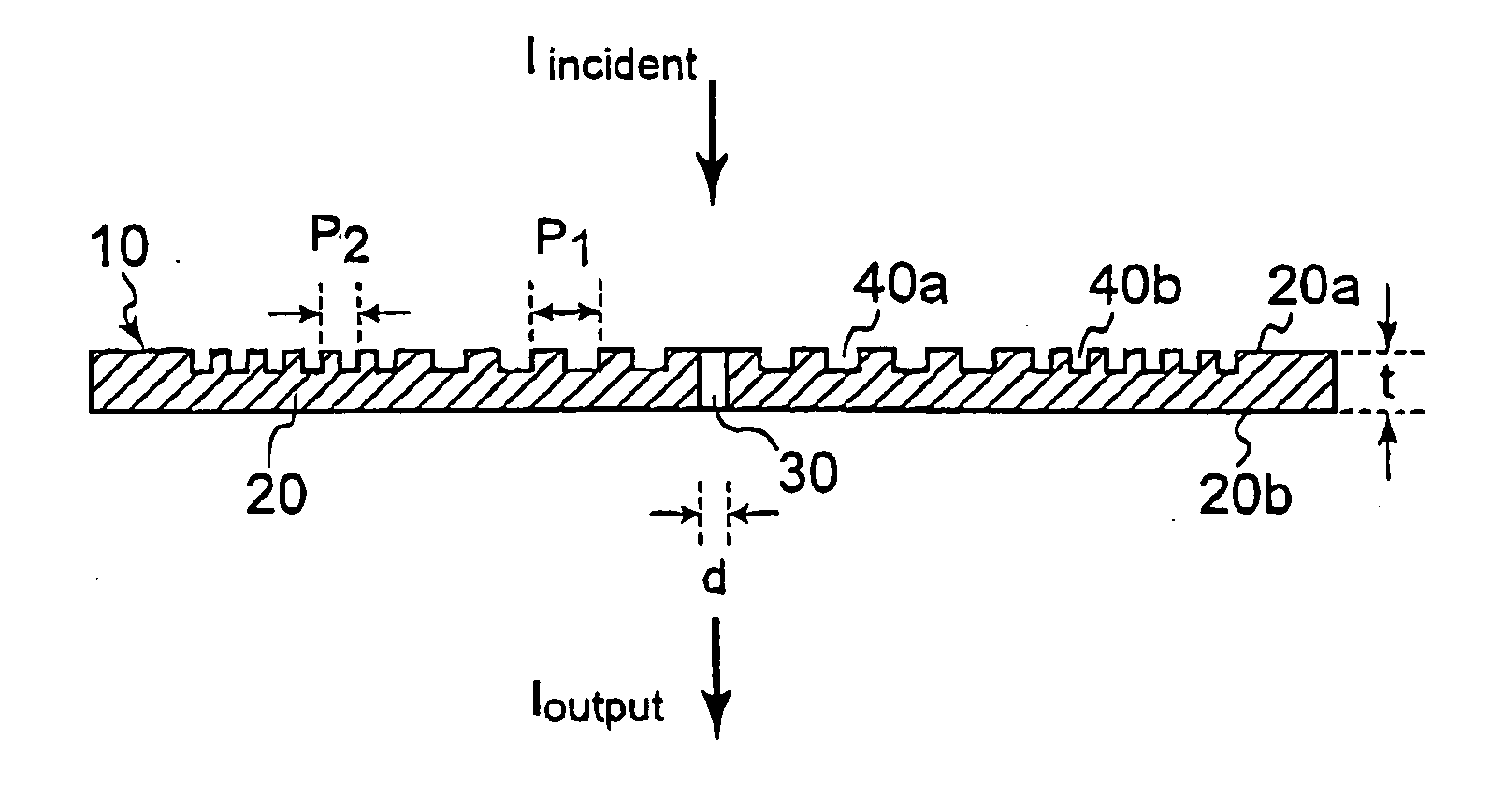
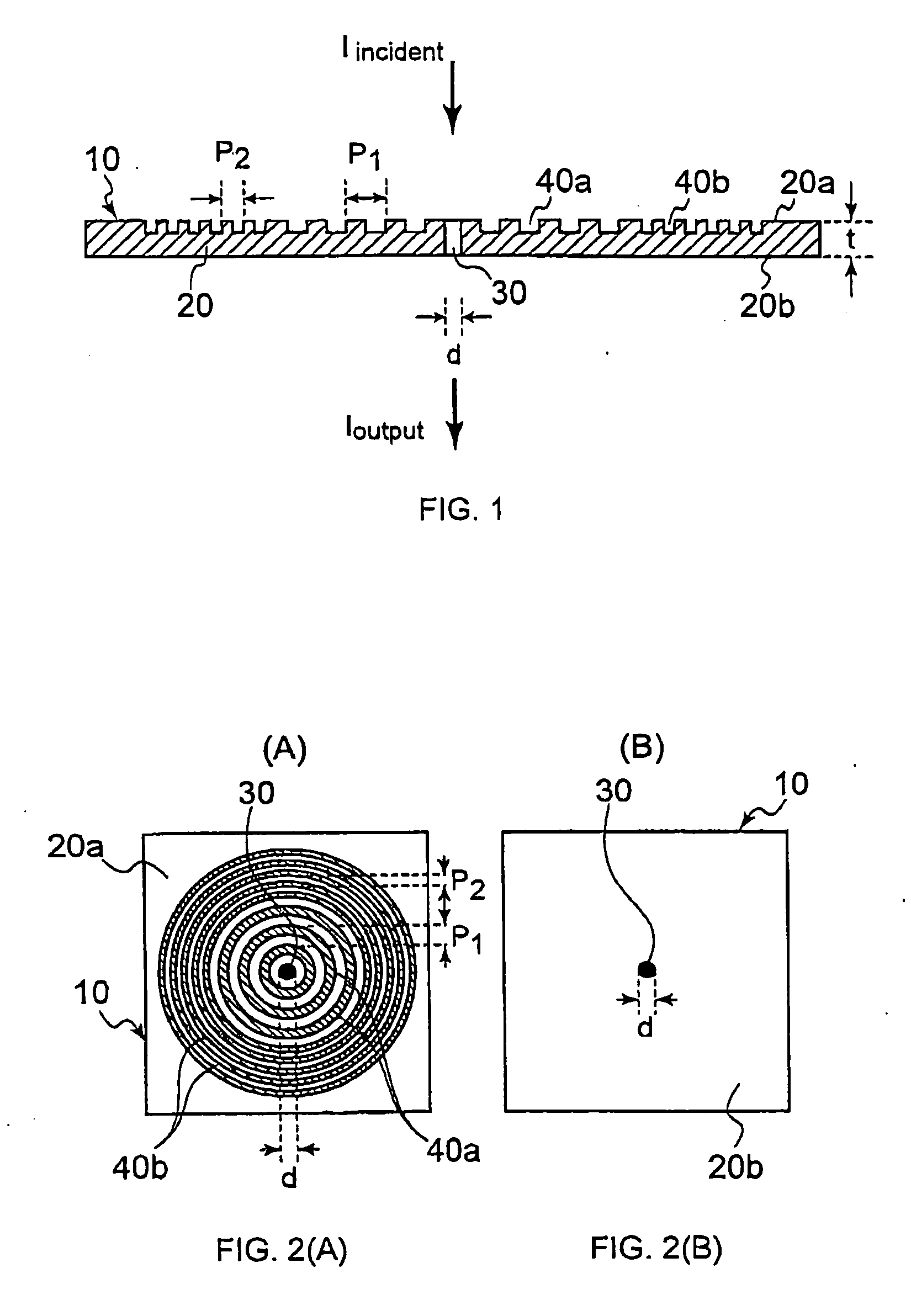
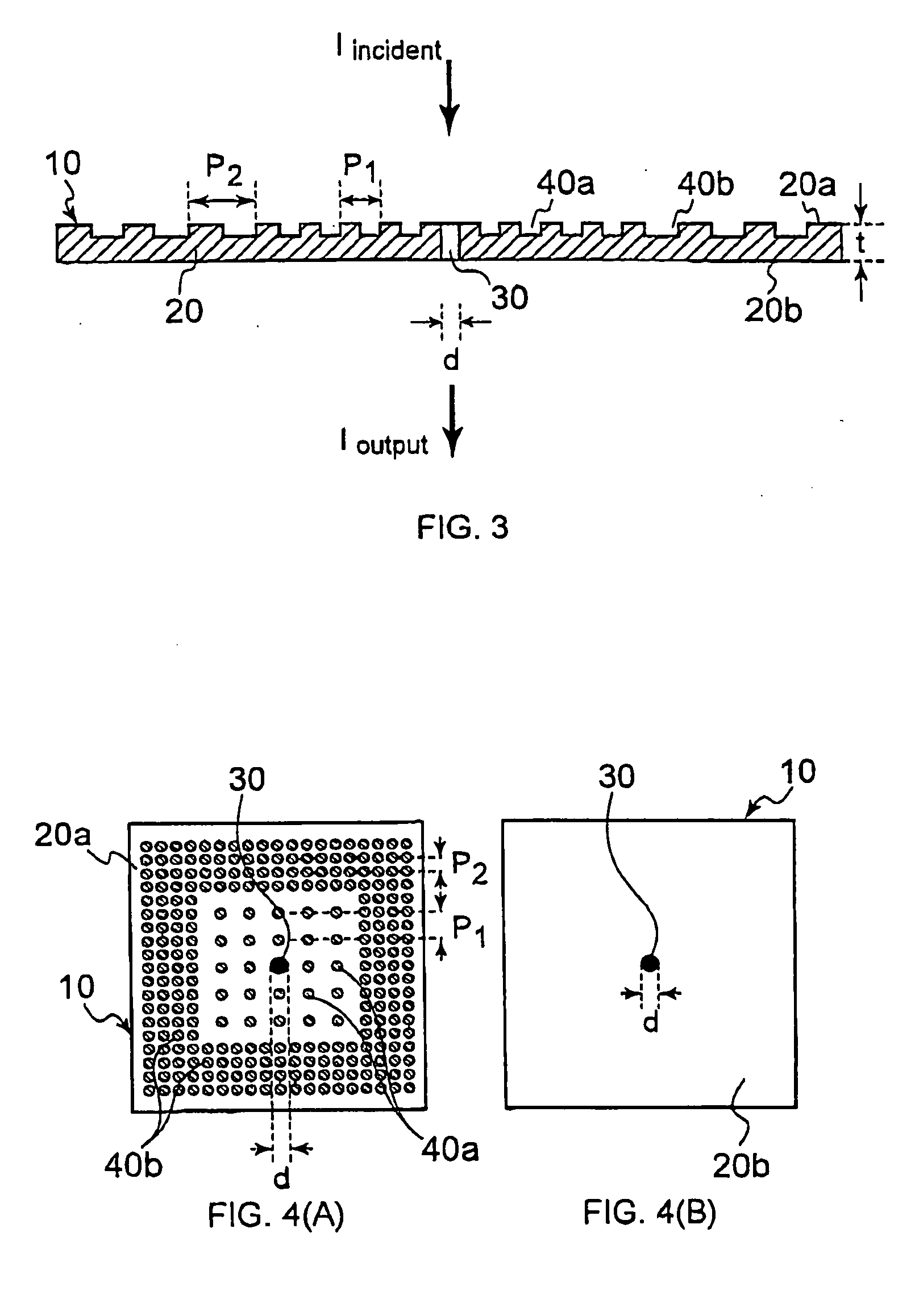
[0062]FIGS. 1, and 2(A) and (B) are diagrams showing an optical device 10 in a first embodiment of the present invention. The optical device 10 has a conductive thin film 20 including a first surface 20a and a second surface 20b. The first surface 20a of the conductive thin film 20 is irradiated with incident light. The conductive thin film 20 has at least one hole whose diameter is d, that is, an opening 30. The conductive thin film 20 is made of a metal or a doped semiconductor material, and aluminum, silver, gold, chromium or the like is preferable. In a case where light of a visible light region is used as incident light, silver is preferable from a viewpoint of optical loss, but the material is not necessarily limited to silver.

[0063] The conductive thin film 20 is provided with a first periodic surface pattern 40a in at least one of the first surface 20a and the second surfac...

embodiment 2

[0093] Next, a second embodiment of the present invention will be described with reference to FIGS. 11 to 13.

[0094]FIG. 11 is a diagram showing an optical device 10 of the present embodiment. The optical device 10 has a conductive thin film 20 including a first surface 20a and a second surface 20b. The first surface 20a of the conductive thin film 20 is irradiated with incident light. The conductive thin film 20 has at least one hole having a diameter d, that is, an opening 30.

[0095] The conductive thin film 20 is provided with a third periodic surface pattern 40c on the second surface 20b of the conductive thin film 20. Here, a reason why the periodic surface pattern 40c formed on the second surface 20b is referred to as the third periodic surface pattern is that the pattern can be combined with the first and second periodic surface patterns 40a and 40b shown in FIG. 1 or 3 as shown in FIG. 12 or 13. A period length P3 of the third periodic surface pattern 40c is the odd time(s) ...

embodiment 3

[0116]FIG. 17 shows one embodiment of an optical head constituted using an optical device of the present invention.

[0117] An “optical recording medium” used in description of the present embodiment means an arbitrary medium with respect to which data is written or read using light, but the present invention is not limited to a phase change medium, a magnetic optical medium, and a dyestuff medium. When the medium is a magnetic optical medium, writing is optically performed, and reading is performed magnetically, not optically in some case.

[0118] An optical head 200 in FIG. 17 is formed into a slider shape for floating the optical head at a predetermined height by rotation of an optical recording medium 150. Laser light emitted from laser 80 is introduced via an optical fiber 100, and collimated by disposing a collimator lens 60 constituted of a micro lens. Furthermore, the collimated light changes its optical path at right angles by a total reflection mirror 70, and the light is fu...


PUM

PropertyMeasurementUnit
thicknessaaaaaaaaaa
period lengthaaaaaaaaaa
depthaaaaaaaaaa

Abstract

A conductive thin film has first and second surfaces and at least one opening extending through from the first surface to the second surface. At least on one of the first and second surfaces, first and second periodic surface patterns having different period lengths are provided. The period length of the second periodic surface pattern is substantially equal to an odd integral multiple of a half of the period length of the first periodic surface pattern. With this, surface plasmon polaritons excited by the first periodic surface pattern undergo odd-order Bragg reflection by the second periodic surface pattern. As a result, the intensity of the light falling on the first surface and transmitted to the second surface through the opening is increased with high efficiency.

Description

TECHNICAL FIELD [0001] The present invention relates to an optical device, more particularly to an optical device provided with a conductive thin film including an opening having a diameter which is not more than a wavelength of incident light and a periodic surface pattern, the optical device being capable of achieving a very high throughput. BACKGROUND ART [0002] An optical recording medium such as a compact disk read only memory (CD-ROM), a digital video disk, or a digital versatile disk (DVD) has features such as a high recording density, a compact design, portability, and tenacity. Additionally, not only a price of the medium itself but also a price of a recording and reproducing device are decreasing. Therefore, the medium increasingly becomes an attractive data storage medium. Moreover, in this type of optical recording medium, there is a demand for a higher recording density in order to make possible the recording of video data for a longer time. [0003] To increase the recor...

Claims


Application Information

Patent Timeline
Patent Type & Authority Applications(United States)
IPC IPC(8): G02B26/08C23C26/00G02B1/10G03B21/56
CPCY10T428/12694G03B21/56
Inventor ISHIHARA, KUNIHIKOHATAKOSHI, GENICHIOHASHI, KEISHIICHIHARA, KATSUTAROICHIHARA, URARA
Owner NEC CORP
Why Eureka
Try Eureka