Interconnect metallization process with 100% or greater step coverage

a technology of interconnects and metallization processes, applied in vacuum evaporation coatings, sputtering coatings, coatings, etc., can solve problems such as reliability concerns and yield degradation, prior art deposits of too much barrier material than is required, and comformality and step coverage problems, etc., to improve the technology extendibility of the semiconductor industry and thin barrier materials

Inactive Publication Date: 2007-11-08
IBM CORP
View PDF15 Cites 40 Cited by
  • Summary
  • Abstract
  • Description
  • Claims
  • Application Information

AI Technical Summary

Benefits of technology

[0008] The present invention provides an interconnect structure with a thicker barrier material coverage at the sidewalls of a feature as compared to the thickness of said barrier material at the feature bottom as well as a method of fabricating such an interconnect structure. The interconnect structure of the present invention has improved technology extendibility for the semiconductor industry as compared with prior art interconnect structure in which the barrier material is formed by a conventional PVD process, a conventional ionized plasma deposition, CVD or ALD. In accordance with the present invention, an interconnect structure having a barrier material thickness at the feature sidewalls (wt) greater than the barrier material thickness at the feature bottom (ht) is provided. That is, the wt / ht ratio is equal to, or greater than, 100% in the inventive interconnect structure.

Problems solved by technology

However, with decreasing critical dimension (CD), it is expected that PVD based deposition techniques will run into comformality and step coverage issues.
These, in turn, will lead to fill issues at plating such as, for example, center and edge voids, which cause reliability concerns and yield degradation.
Also, in order to meet the minimum amount of barrier material at the feature sidewalls, the prior art deposits too much barrier material than is required at the feature bottom.
This increased liner volume fraction reduces the total available volume fraction for the conductive material, i.e., Cu, inside the feature, and degrades the total circuit performance.
The ionized plasma deposition process described above thus always provides too much barrier material at the feature bottom, which is not desired for electrical resistance reduction on advanced semiconductor products.

Method used


Image

  • Interconnect metallization process with 100% or greater step coverage
  • Interconnect metallization process with 100% or greater step coverage
  • Interconnect metallization process with 100% or greater step coverage

Examples


Embodiment Construction

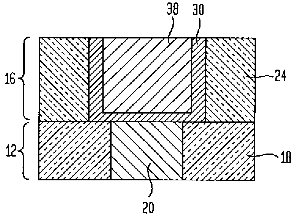
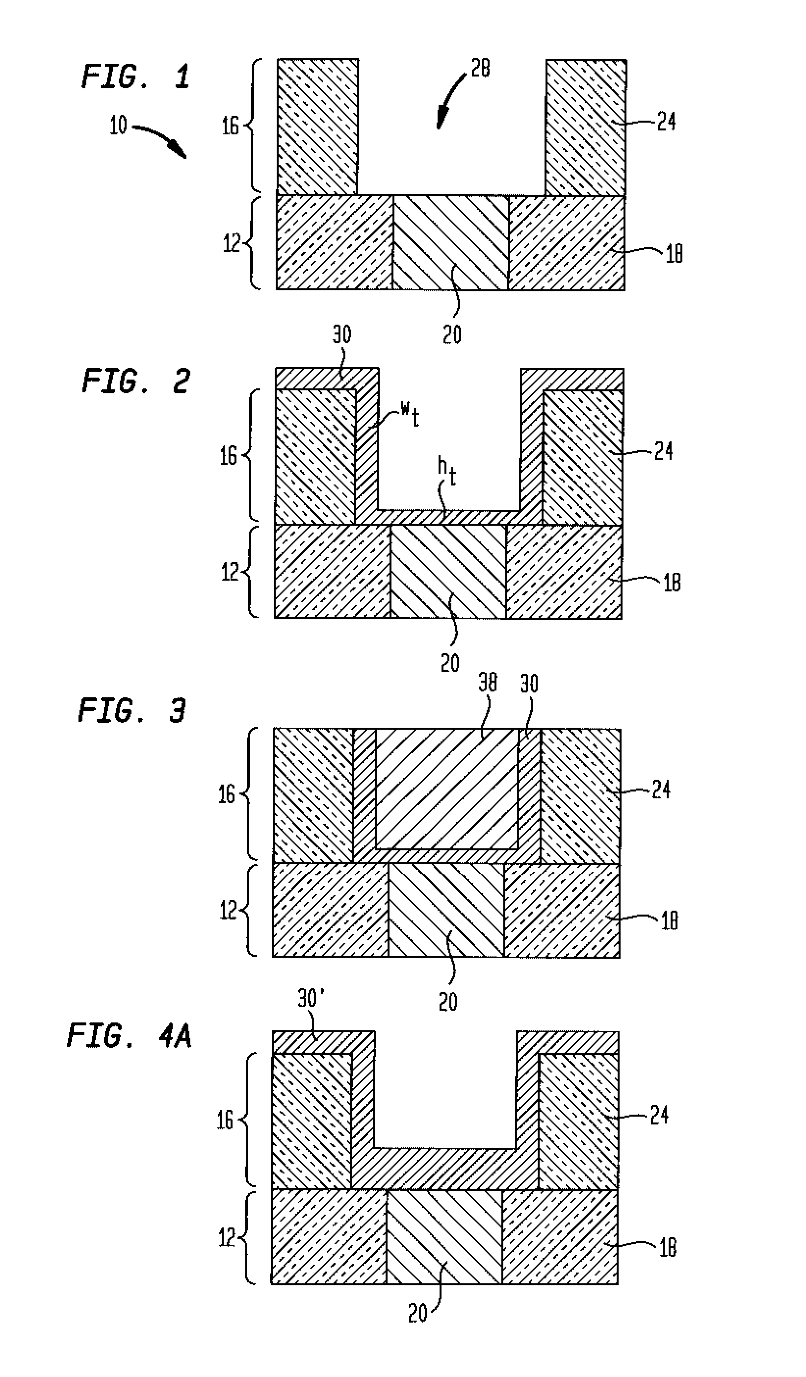
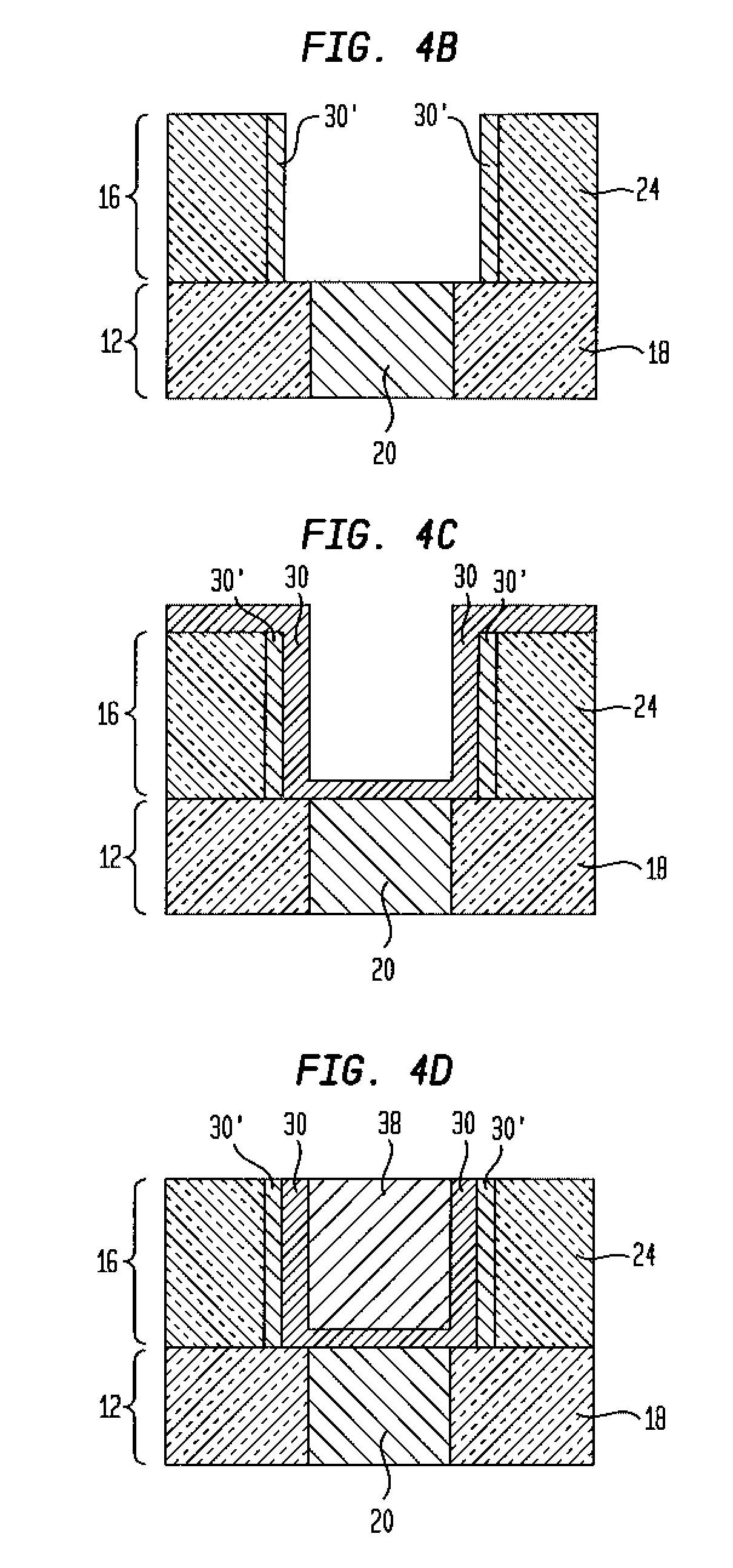
[0025] The present invention, which provides an interconnect structure having at least a barrier material with equal to, or greater than, 100% step coverage and a method of fabricating such an interconnect structure, will now be described in greater detail. The drawings of the present application, which are referred to herein below in greater detail, are provided for illustrative purposes and, as such, they are not drawn to scale.

[0026] The process flow of the present invention begins with providing the initial interconnect structure 10 shown in FIG. 1. Specifically, the initial interconnect structure 10 shown in FIG. 1 comprises a multilevel interconnect including a lower interconnect level 12 and an upper interconnect level 16 that, in some embodiments, are separated in part by dielectric capping layer (not shown). The lower interconnect level 12, which may be located above a semiconductor substrate including one or more semiconductor devices, comprises a first dielectric materia...


PUM

PropertyMeasurementUnit
dielectric constantaaaaaaaaaa
thicknessaaaaaaaaaa

Abstract

An interconnect structure with a thicker barrier material coverage at the sidewalls of a feature as compared to the thickness of said barrier material at the feature bottom as well as a method of fabricating such an interconnect structure are provided. The interconnect structure of the present invention has improved technology extendibility for the semiconductor industry as compared with prior art interconnect structure in which the barrier material is formed by a conventional PVD process, a conventional ionized plasma deposition, CVD or ALD. In accordance with the present invention, an interconnect structure having a barrier material thickness at the feature sidewalls (wt) greater than the barrier material thickness at the feature bottom (ht) is provided. That is, the wt / ht ratio is equal to, or greater than, 100% in the inventive interconnect structure.

Description

FIELD OF THE INVENTION [0001] The present invention relates to a semiconductor structure and a method of fabricating the same. More particularly, the present invention relates to an interconnect structure of the single or dual damascene type in which the step coverage of at least the barrier material within a feature provided in a dielectric material is equal to, or greater than, 100%. The present invention also relates to a method of fabricating such a semiconductor structure. BACKGROUND OF THE INVENTION [0002] Generally, semiconductor devices include a plurality of circuits which form an integrated circuit fabricated on a semiconductor substrate. A complex network of signal paths will normally be routed to connect the circuit elements distributed on the surface of the substrate. Efficient routing of these signals across the device requires formation of multilevel or multilayered schemes, such as, for example, single or dual damascene wiring structures. The wiring structure typical...

Claims


Application Information

Patent Timeline
Patent Type & Authority Applications(United States)
IPC IPC(8): H01L21/4763
CPCC23C14/046H01L21/2855H01L21/76846H01L21/76844H01L21/76843
Inventor YANG, CHIH-CHAOCHANDA, KAUSHIK
Owner IBM CORP
Why Eureka
Try Eureka