Manufacturing method and manufacturing apparatus for image display device

a manufacturing apparatus and image display technology, applied in the manufacture of electrode systems, tubes with screens, electric discharge tubes/lamps, etc., can solve the problems of unfavorable electrical conductive sealing material sealing work, unstable coupling of substrates, and unnecessary gas production, and achieve quick and stable sealing work. effect of electrical conductive sealing material

Inactive Publication Date: 2007-11-08
ENOMOTO TAKASHI +2
View PDF3 Cites 2 Cited by
  • Summary
  • Abstract
  • Description
  • Claims
  • Application Information

AI Technical Summary

Benefits of technology

[0015] The present invention has been made in consideration of the above-described problems, and the object of the invention is to provide a manufacturing method for an image display device, which enables a quick and stable sealing work of an electrically conductive sealing material.
[0019] According to the manufacturing method for the image display device with the above structure, an electric current, which has such a gentle curve that the current reaches a maximum current value after a current-increasing period of 10% or more of the entire power-supply time, is supplied to the electrically conductive sealing material for a predetermined time period, thus heating / melting the sealing material and carrying out the sealing process. Thereby, the maximum current value for heating / melting is set at a value twice as high as a value in the prior art. Hence, even in the case where the power-supply time for heating is reduced, the occurrence of spark can surely be avoided, and the current can stably be supplied to the sealing layer. Thereby, the sealing layer can be formed with uniform thickness over the entire periphery, and the sealing work can stably be performed in a short time while the entire substrate is kept at low temperatures.

Problems solved by technology

However, when frit glass is sintered, unnecessary gas is produced.
The gas remains in the sealed envelope after fusion, and the gas causes a problem when the inside of the envelope is evacuated later to a high vacuum level.
If the sealing material is not stably melted, the time for melting the sealing material varies from envelope to envelope, and stable coupling of the substrates cannot be carried out.
If the electrically conductive sealing material is excessively heated, such problems arise that the sealing material may be broken due to heat or a crack may occur in the substrates.
Conversely, if the sealing material is not sufficiently melted, the coupling of the substrates becomes deficient, and such problems arise that the air-tightness for maintaining vacuum deteriorates or the vacuum state of the envelope cannot be kept.
Although the time for melting and cooling the electrically conductive sealing material can be reduced by increasing the value of the constant current, the increase in current value leads to frequent occurrence of sparks between the sealing material and the electrode, between the electrode and the apparatus-side electrode contact, or between the sealing layers, and there arises the problem that the sealing layer cannot stably be melted.
In addition, in the above-described manufacturing method, only one side of the substrate, to which the indium is applied, is heated by the power-supply heating, resulting in a difference in temperature between the front and back surfaces of the substrate.
If the envelope becomes partly thick, such problems arise that the air-tightness for vacuum deteriorates, the relative position between the electron source and phosphor layer is displaced at the corner part, and the envelope cannot easily be attached to the cabinet.

Method used


Image

  • Manufacturing method and manufacturing apparatus for image display device
  • Manufacturing method and manufacturing apparatus for image display device
  • Manufacturing method and manufacturing apparatus for image display device

Examples


first embodiment

[0051] An FED, which is an image display device, and a manufacturing method of the FED according to the present invention will now be described in detail with reference to the accompanying drawings.

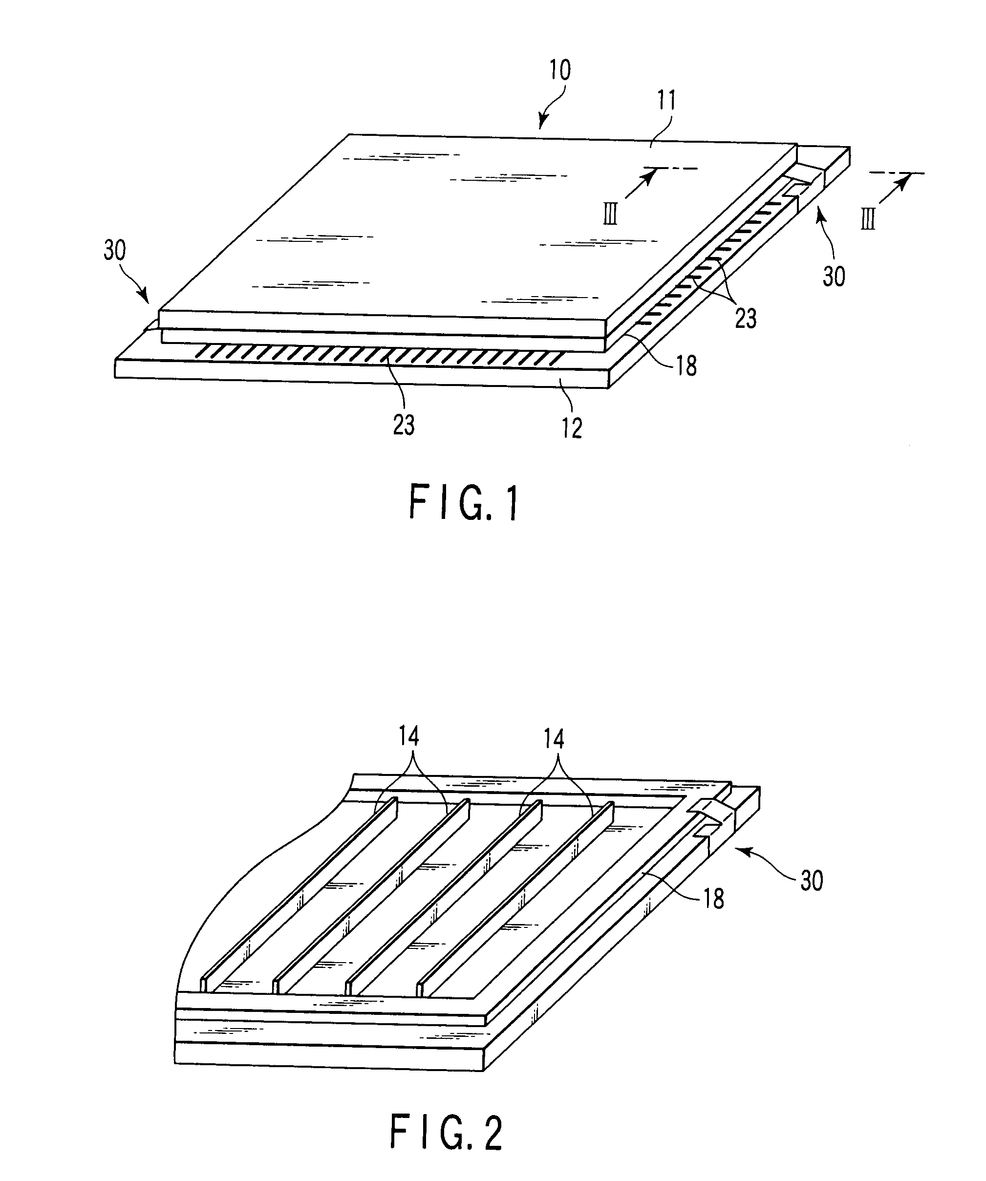
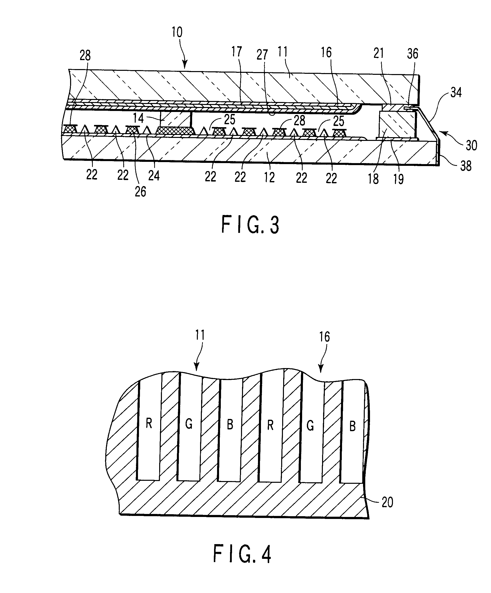
[0052] As shown in FIG. 1 to FIG. 4, the FED includes a front substrate 11 and a rear substrate 12, each of which is formed of a rectangular glass plate. The front substrate 11 and rear substrate 12 are disposed to be opposed to each other with a gap of 1 to 2 mm. The rear substrate 12 has a greater size than the front substrate 11. Peripheral edge parts of the front substrate 11 and rear substrate 12 are attached via a rectangular-frame-shaped side wall 18, thereby forming a flat, rectangular vacuum envelope 10 in which a vacuum is maintained.

[0053] A plurality of plate-shaped support members 14 are provided within the vacuum envelope 10 in order to support an atmospheric pressure load acting on the front substrate 11 and rear substrate 12. The support members 14 extend in a direction p...

second embodiment

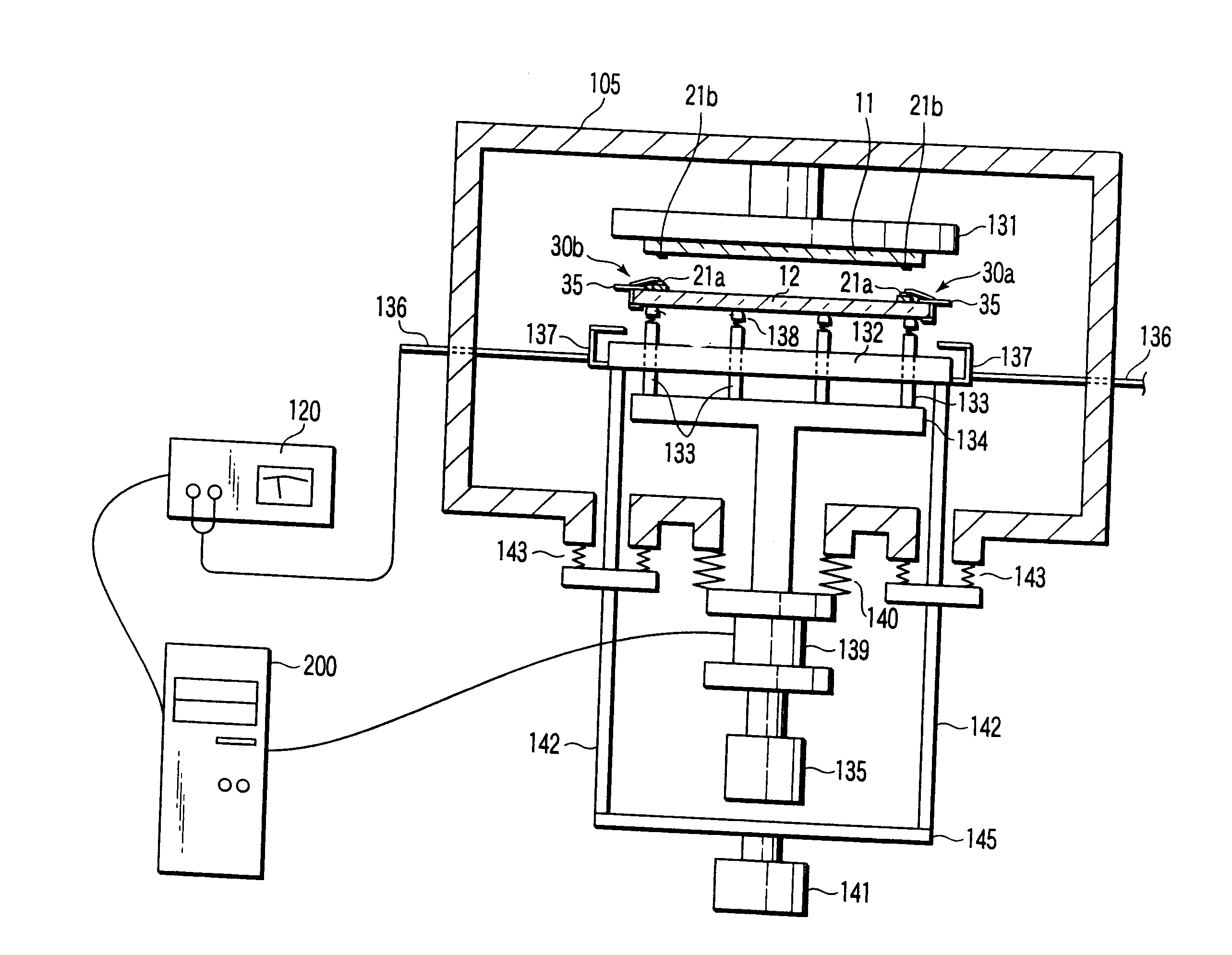
[0107] In the second embodiment, the power supply is executed in the state in which the front substrate and rear substrate are pressed on each other and the sealing layers are put in contact. Alternatively, after the sealing layer of the front substrate and the sealing layer of the rear substrate are supplied with power and heated and melted, the substrates may be pressed toward each other and sealed together. In this case, the two pairs of electrodes are mounted on the rear substrate, and one pair of electrodes are formed such that their contact portions contact the rear substrate-side sealing layer and the other pair of electrodes are formed such that their contact portions contact the front-substrate-side sealing layer.

[0108] In the second embodiment, the electrodes 30a and 30b are pushed upward by the power supply electrodes 137. Alternatively, the corner portions of the rear substrate may directly be pushed by a pushing mechanism that is separately provided on the assembly cham...


PUM


Abstract

After sealing layers are formed on peripheral edge parts of a front substrate and a rear substrate, the front substrate and the rear substrate are disposed to be opposed to each other. Current paths are formed in the sealing layers, and power supply is begun. An electric current, which reaches a maximum current value after a current-increasing period of 10% or more of an entire power-supply time, is supplied for a predetermined time period. The sealing layers are heated and melted by the power supply, and peripheral parts of the front substrate and rear substrate are joined.

Description

CROSS-REFERENCE TO RELATED APPLICATIONS [0001] This application is a Divisional of and claims the benefit of priority under 35 U.S.C. § 120 from U.S. Ser. No. 11 / 510,643, filed Aug. 28, 2006, which is a Continuation application of PCT Application No. PCT / JP2005 / 003339, filed Feb. 28, 2005, which was published under PCT Article 21(2) in Japanese. [0002] This application is based upon and claims the benefit of priority from prior Japanese Patent Applications No. 2004-057954, filed Mar. 2, 2004; and No. 2004-068056, filed Mar. 10, 2004, the entire contents of both of which are incorporated herein by reference.BACKGROUND OF THE INVENTION [0003] 1. Field of the Invention [0004] The present invention relates to a manufacturing method and a manufacturing apparatus for a flat image display device including a pair of substrates which are opposed to each other and are attached to each other at their peripheral edge parts. [0005] 2. Description of the Related Art [0006] In recent years, variou...

Claims


Application Information

Patent Timeline
Patent Type & Authority Applications(United States)
IPC IPC(8): H01J9/26H01J29/86H01J31/12
CPCH01J9/261
Inventor ENOMOTO, TAKASHIYAMADA, AKIYOSHIYOKOTA, MASAHIRO
Owner ENOMOTO TAKASHI
Why Eureka
Try Eureka