Liquid crystal display device

a liquid crystal display and display screen technology, applied in static indicating devices, non-linear optics, instruments, etc., can solve the problem of not considering the rubbing direction of alignment films, and achieve the effect of reducing the tim

Inactive Publication Date: 2007-11-29
JAPAN DISPLAY CENT INC
View PDF8 Cites 12 Cited by
  • Summary
  • Abstract
  • Description
  • Claims
  • Application Information

AI Technical Summary

Benefits of technology

[0012]The present invention has been made in consideration of the above-described problems, and the object of...

Problems solved by technology

In the above-described liquid crystal display device, however, no co...

Method used


Image

  • Liquid crystal display device
  • Liquid crystal display device
  • Liquid crystal display device

Examples


first embodiment

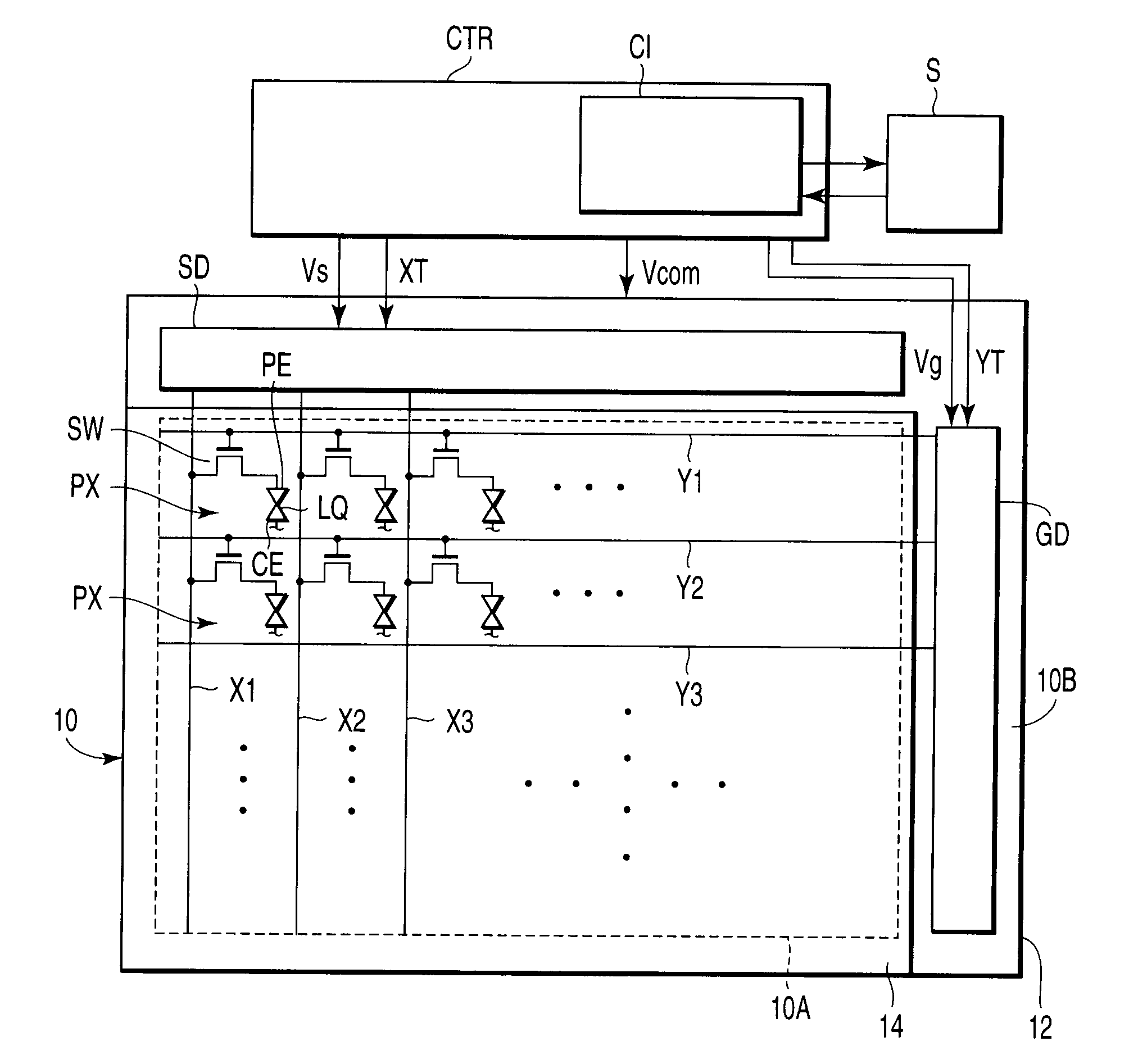
[0038]A liquid crystal display device according to the present invention will now be described with reference to the accompanying drawings. As shown in FIG. 1, the liquid crystal display device according to this embodiment includes a substantially rectangular, flat liquid crystal display panel 10. The liquid crystal display panel 10 includes a pair of mutually opposed substrates, i.e. an array substrate 12 and a counter-substrate 14. A liquid crystal layer LQ is held between the array substrate 12 and counter-substrate 14.

[0039]The liquid crystal display panel 10 includes a display section 10A which is composed of a plurality of display pixels PX that are arrayed in a matrix, and a peripheral section 10B which is provided around the display section 10A.

[0040]In the display section 10A, a plurality of scanning lines Y (Y1 to Ym) are disposed along the rows in which the plural display pixels PX are arranged, and a plurality of signal lines X (X1 to Xn) are disposed along the columns i...

third embodiment

[0065]Next, the present invention is described with reference to the accompanying drawings.

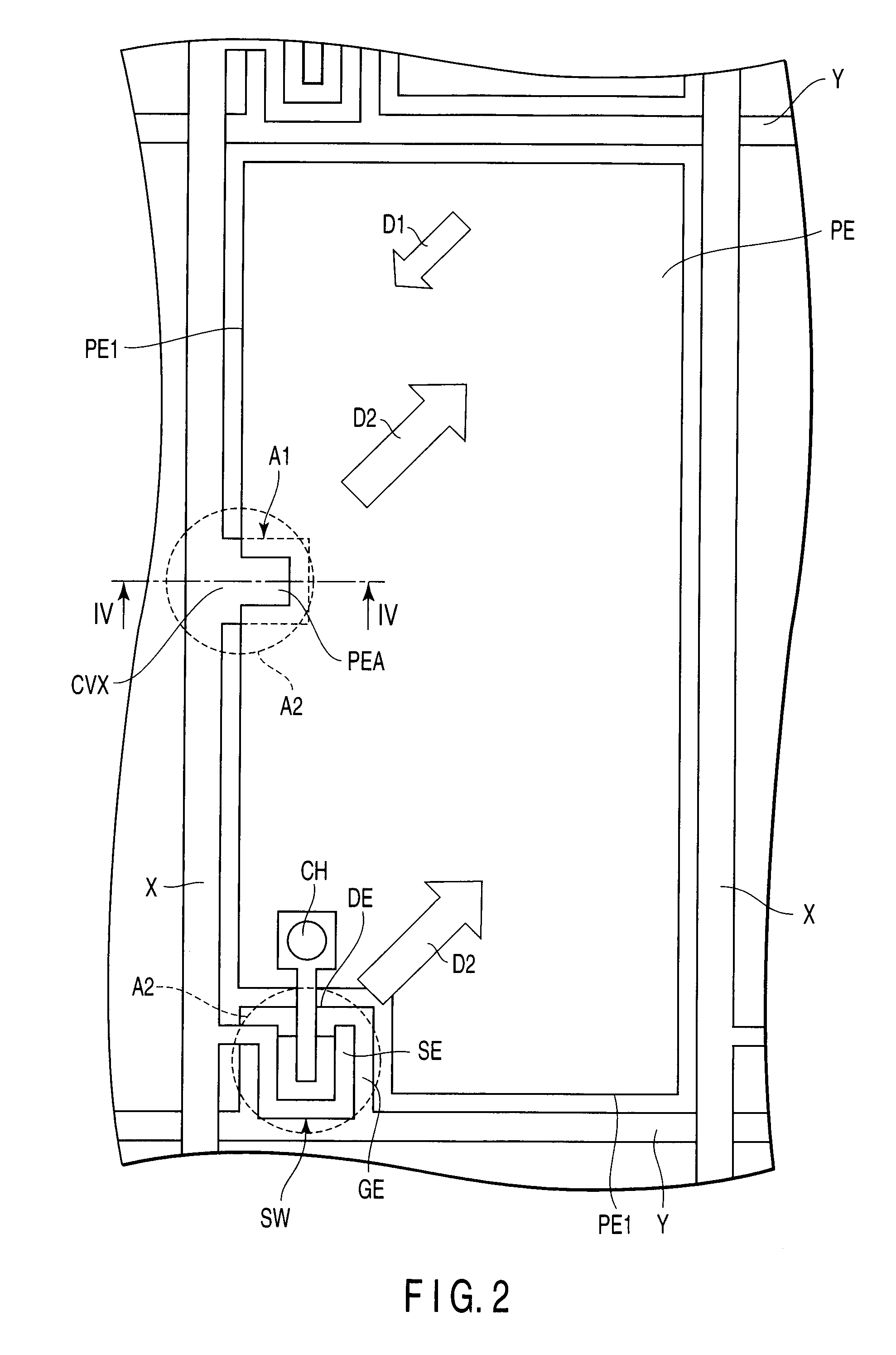
[0066]Like the above-described liquid crystal display device of the first embodiment, the liquid crystal display device according to the present third embodiment includes a transition-nucleus formation section A1 on a terminal-end side of the rubbing direction D1 in each display pixel PX. Specifically, in the liquid crystal display device of the present embodiment, the transition-nucleus formation section A1 is provided at a side edge portion PE1 on the terminal-end side of the rubbing direction D1 of the alignment film, which corresponds to a long side of the rectangular display pixel PX.

[0067]The transition-nucleus formation section A1 is composed of a recess portion PEA of the pixel electrode PE, and a wiring line, namely, a storage capacitance line Cs, which is partly opposed to the recess portion PEA via an insulation layer and has a potential different from the potential of the pixel ele...


PUM


Abstract

A liquid crystal display device of an OCB mode includes a liquid crystal layer held between an array substrate and a counter-substrate, and a display section composed of display pixels arrayed in a matrix. The array substrate includes pixel electrodes which are disposed in association with the display pixels. The counter-substrate includes a counter-electrode opposed to the pixel electrodes. The substrates include a pair of alignment films which are disposed on the pixel electrodes and the counter-electrode, respectively, and are subjected to rubbing treatment to control an alignment state of liquid crystal molecules included in the layer. A transition-nucleus formation section, which generates an electric field for transitioning the alignment state of the liquid crystal molecules included in the layer from a non-display state to a display state, is provided on a terminal-end side of a rubbing direction of each of the alignment films in each of the display pixels.

Description

CROSS-REFERENCE TO RELATED APPLICATIONS[0001]This application is based upon and claims the benefit of priority from prior Japanese Patent Application No. 2006-146447, filed May 26, 2006, the entire contents of which are incorporated herein by reference.BACKGROUND OF THE INVENTION[0002]1. Field of the Invention[0003]The present invention relates generally to a liquid crystal display device, and more particularly to an active-matrix liquid crystal display device.[0004]2. Description of the Related Art[0005]In general, a liquid crystal display device includes a liquid crystal display panel having a display section which is composed of display pixels that are arrayed in a matrix. The liquid crystal display panel includes a pair of mutually opposed substrates, i.e. an array substrate and a counter-substrate, and a liquid crystal layer which is held between the paired substrates.[0006]The array substrate includes pixel electrodes which are disposed in association with the plural display p...

Claims


Application Information

Patent Timeline
IPC IPC(8): G09G3/36G02F1/1343
CPCG02F1/133784G02F1/1362G02F1/1395G09G2330/026G09G2300/0491G09G2320/0252G09G2320/041G09G3/3651
Inventor FUKAMI, TETSUOTSUKANE, MIDORINAKAO, KENJI
Owner JAPAN DISPLAY CENT INC
Why Eureka
Try Eureka