[0049]Hereinafter, embodiments of the present invention will be described with reference to the drawings.
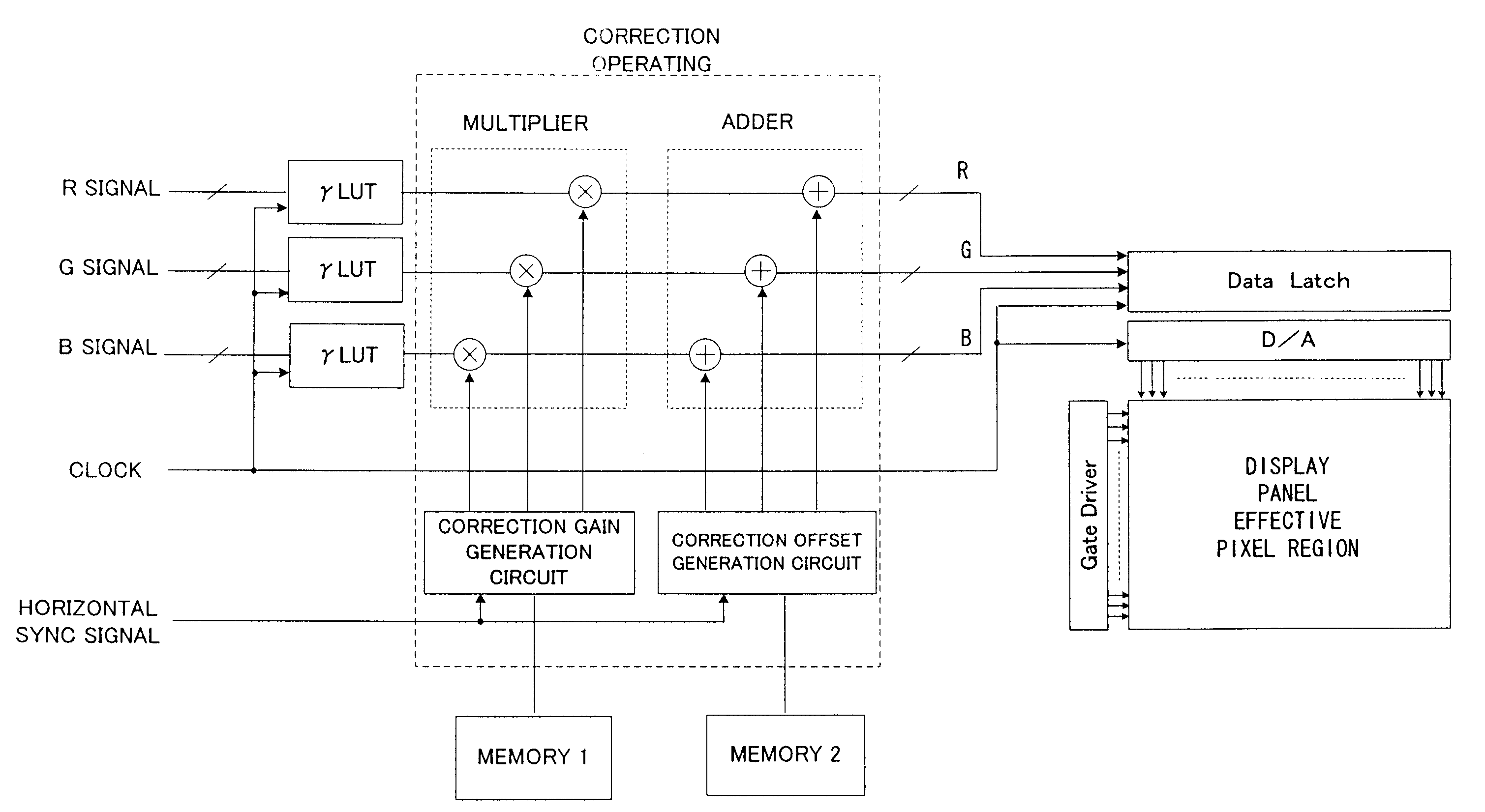
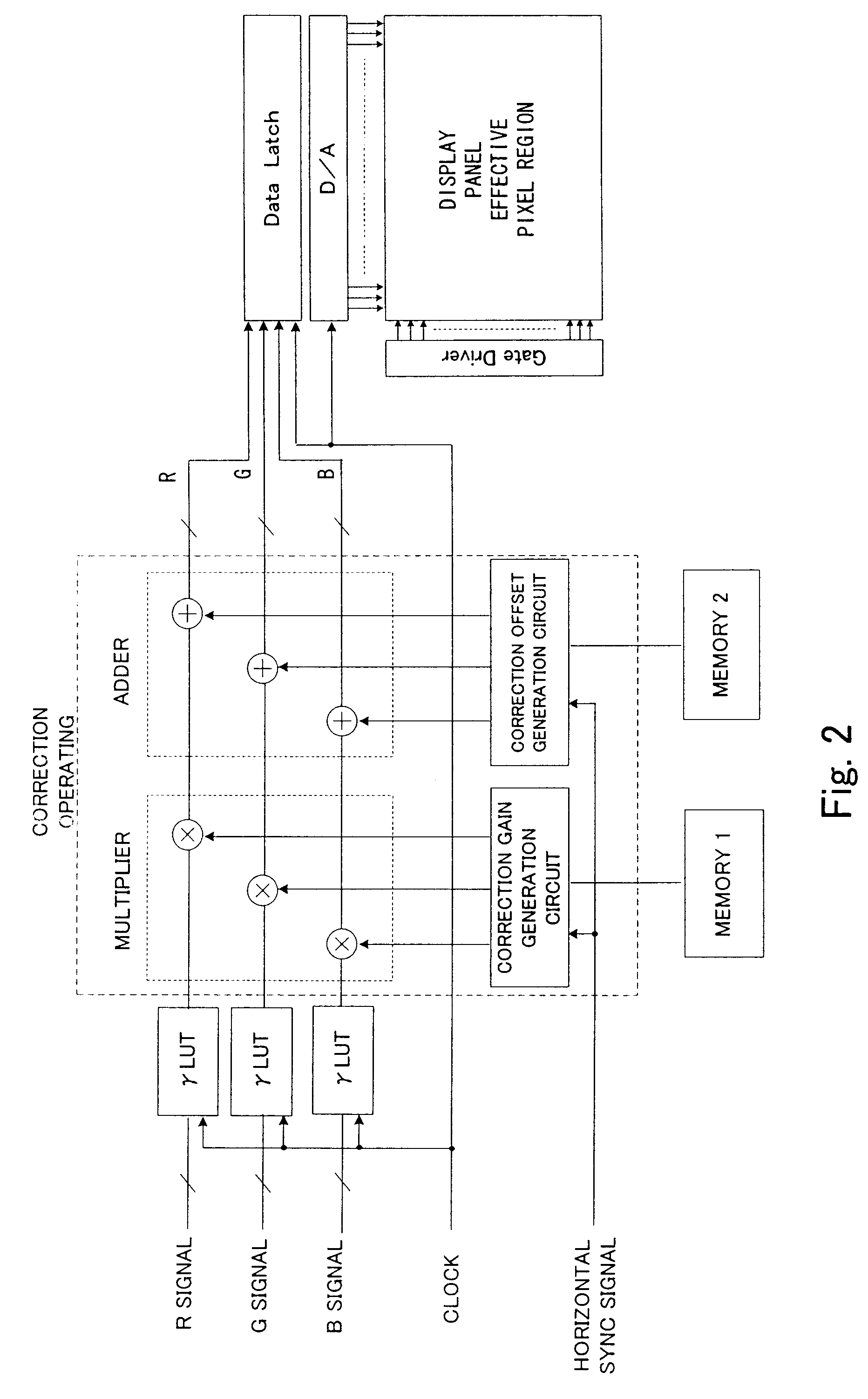
[0050]FIG. 4 shows an example of an organic EL display apparatus according to the present invention, which can produce corrected brightness data, i.e., analog signals, based on input brightness data and can supply the corrected brightness data to pixels constituting a display panel.
[0051]A display panel 10 includes numerous R, G, and B pixels (i.e., pixels generating R, G, and B colors), and can input R, G, and B brightness signals for the display of R, G, and B colors. For example, the display panel 10 includes the same color of pixels arrayed in the vertical direction. One of R, G, and B data can be supplied to each data line. Each pixel can emit light in response to one of R, G, and B data supplied from a corresponding data line. In the example, R, G, and B signals are 8-bit brightness data.
[0052]The R, G, and B signals can be independently supplied to corresponding R, G, and B look-up tables LUT20. Each of the R, G, and B look-up table LUT20 stores gamma correction data for obtaining a desired relationship (i.e., desired curve) between the light-emitting brightness (i.e., driving current) and the brightness data, with reference to average values of the offset and the gain of the display panel 10. In other words, each look-up table 20 can store correction data for compensating the characteristics (a) shown in FIG. 1.
[0053]Instead of using the look-up tables LUT20, the display apparatus can store predetermined equations to calculate conversion values of the brightness data.
[0054]Each look-up table LUT20 receives a pixel clock in synchronism with an input signal of each pixel and produces an output in synchronism with the pixel clock.
[0055]The R, G, and B look-up tables LUT20 can supply their outputs to corresponding R, G, and B multipliers 22. A correction gain generation circuit 24 can supply gain correction values to the R, G, and B multipliers 22, respectively.
[0056]The R, G, and B multipliers 22 can supply their outputs to corresponding R, G, and B adders 28. A correction offset generation circuit 30 can supply offset correction values to the R, G, and B adders 28, respectively.
[0057]The R, G, and B adders 28 can supply their outputs to a data latch circuit 32. The data latch circuit 32 can supply latched data to a D/A converter 34. The D/A converter 34 can convert the R, G, and B digital signals into corresponding analog signals, and can supply the converted signals to corresponding data lines of the display panel 10.
[0058]Thus, the corrected data signals are supplied via the data lines to pixel positions of respective colors, so that the EL element in each pixel can be driven based on current corresponding to a given data signal.
[0059]As described above, in the present embodiment, the look-up table LUT20 compensates the offset and the V-I characteristics of an average driver TFT and performs the gamma correction. The correction gain generation circuit 24 and the correction offset generation circuit 30 generate a correction gain and a correction offset for each pixel positioned in the display panel 10.
[0060]Therefore, the display apparatus of the present embodiment not only compensates a deviation AVth of the threshold voltage Vth for the driving transistor (driver TFT) in each pixel but also compensates the V-I characteristics representing the relationship between the gate-source voltage Vgs and the drain current (i.e., driving current of the organic EL). Thus, the driving current corresponding to the brightness data can be appropriately supplied to the organic EL element.
[0061]In the present embodiment, the correction gain generation circuit 24 is connected via an expansion circuit 36 to a memory 38. The correction gain generation circuit 24 has a fundamental function of generating a gain correction value adaptive to the input brightness data with reference to a pixel position on the screen. To this end, the correction gain generation circuit 24 reads necessary correction data from the memory 38 and determines the gain correction value. The memory 38 stores entropy coded data. The expansion circuit 36 expands the entropy coded data and supplies expanded correction data to the correction gain generation circuit 24.
[0062]Furthermore, the correction offset generation circuit 30 is connected via an expansion circuit 40 to a memory 42. The correction offset generation circuit 30 has a fundamental function of generating an offset correction value adaptive to the input brightness data with reference to a pixel position on the screen.
[0063]To this end, the correction offset generation circuit 30 reads necessary correction data from the memory 42 and determines the offset correction value. The memory 42 stores entropy coded data. The expansion circuit 40 expands the entropy coded data and supplies expanded correction data to the correction offset generation circuit 30.
[0064]In general, the brightness irregularities are classified into various types according to their causes or sources. For example, the dispersion of correction values can generate irregularities. However, as shown in FIGS. 3A and 3B, an ordinary histogram of correction values has a distribution pattern having a largest value at 0 and other values decreasing according to the absolute value of the irregularities. Hence, the display apparatus of the present embodiment compresses the correction data by entropy coding and stores the entropy coded data (i.e., compressed correction data) in the memories 38 and 42.
[0065]When the input R, G, and B signals are displayed on the display panel 10, the expansion circuits 36 and 40 expand the compressed correction data while the calculation for correcting the pixel data is performed.
[0066]As one example, the display panel 10 can include 320×240 pixels. The display apparatus performs a simplified correction for correcting only the threshold voltage Vth. It is now assumed that each signal data consists of 6 bits, and the display apparatus can perform correction within the range of ±25% for each signal data. In this case, one pixel requires correction data of 5 bits (−15 to +15) including code bits. Namely, an ordinarily required memory size is 320×240×5=384,000 bits.
[0067]The total data amount, required when the Huffman coding is employed, can be obtained by summing up “bit length of Huffman code×frequency” of respective correction values. Table 1 shows one example of the frequency distribution of irregularities and Huffman codes, according to which the total data amount rises up to 251,205 bits. The required memory size is equal to a sum of the above data amount and the size required for a Huffman table.
TABLE 1 correction code frequency × value frequency Huffman code bit length code bit length 0 21405 00 2 42810 1 10075 010 3 30225 −1 9816 100 3 29448 2 7411 110 3 22233 −2 6808 111 3 20424 −3 5120 0110 4 20480 3 5106 1010 4 20424 −4 2992 01110 5 14960 4 2761 10110 5 13805 5 1379 011110 6 8274 −5 1262 101110 6 7572 −6 955 0111110 7 6685 6 595 1011110 7 4165 7 404 01111110 8 3232 −7 226 10111110 8 1808 −8 128 011111110 9 1152 8 121 101111110 9 1089 −9 97 101111111 9 873 9 63 0111111110 10 630 10 32 01111111110 11 352 −10 23 011111111110 12 276 11 12 0111111111110 13 156 −11 5 01111111111110 14 70 12 2 011111111111110 15 30 −12 1 0111111111111110 16 16 13 1 0111111111111111 16 16 −15 0 — — — −14 0 — — — −13 0 — — — 14 0 — — — 15 0 — — — total 251205
[0068]Furthermore, unless the compression data exceed a maximum memory capacity, the display apparatus of the present embodiment can correct a wide range of irregularities. In other words, according to the example, the conventional method cannot completely correct irregularities, if the irregularities exceed ±25%.
[0069]The display apparatus of the present embodiment can obtain the Huffman codes according to the following general procedure, including the steps of:
[0070]1) arraying a total of n correction values (symbols) in order of frequency;
[0071]2) selecting two symbols that have the lowest and second lowest frequencies, allocating the code 1 or 0 to the selected symbols, and integrating them as a single symbol having a summed-up frequency of two original symbols;
[0072]3) arraying a total of (n−1) symbols resulting from the above processing in order of frequency, selecting two symbols having the lowest and second lowest frequencies, and allocating the code 1 or 0 to the selected symbols; and
[0073]4) repeating the above-described processing until the symbol number reduces to 1, and reading the codes allocated in the process of the above processing in the inverse order to obtain a code of a corresponding symbol.
[0074]The Huffman table obtained by the above-described procedure can be stored together with compressed correction data in the memory of the 10 display apparatus, and can be used in the decoding processing.
[0075]FIG. 5 shows an arrangement for calculating correction values, including a memory 50, a Huffman decoding section 52, and a correction operating section 54. The memory 50 can store a Huffman table and compression data. The Huffman decoding section 52 can read, from the memory 50, correction data adaptive to the input data and produce Huffman decoded correction values. The correction operating section 54 can receive the Huffman decoded correction values from the Huffman decoding section 52. The correction operating section 54 is functionally equivalent to the multiplier 22 or the adder 28 shown in FIG. 4. The memory 50 is functionally equivalent to the memory 38 or 42 shown in FIG. 4. The Huffman decoding section 52 is functionally equivalent to the expansion circuit 36 or 40 shown in FIG. 4.
[0076]FIG. 6 is a Huffman tree showing part of the codes shown in the table 1. Compared to using the table 1, storing a Huffman tree in a memory as described below is convenient because the data can be directly used in the decoding processing.
[0077]First, an arbitrary number is allocated to each node of the tree as shown in FIG. 7, with an exception that 0 is allocated to the root. For each node, the information of the side “1” (i.e., the side numbered with 1) is stored in bits 11 through 6 and the information of the side “0” (i.e., the side numbered with 0) is stored in bits 5 through 0 in a corresponding address of the memory.
[0078]When a leaf is attached to the side “1”, 0 is stored in bit 11 and the data is stored in bits 10 through 6. When a node is attached to the side “1”, 1 is stored in bit 11 and the number of node is stored in bits 10 through 6.
[0079]Similarly, when a leaf is attached to the side “0”, 0 is stored in bit 5 and the data is stored in bits 4 through 0. When a node is attached to the side “0”, 1 is stored in bit 5 and the number of nodes is stored in bits 4 through 0.
[0080]In this case, the data is an integer of 5 bits attached with a code, and the number of nodes is an integer of 5 bits attached with no code.
[0081]Table 2 shows the contents of a memory storing Huffman codes allocated as shown in Table 1.
TABLE 2 Address Bit 11 Bit 10~6 Bit 5 Bit 4~0 0 1 16 1 1 1 1 2 0 0 2 1 3 0 1 3 1 4 0 −3 4 1 5 0 −4 5 1 6 0 5 6 1 7 0 −6 7 1 8 0 7 8 1 9 0 −8 9 1 10 0 9 10 1 11 0 10 11 1 12 0 −10 12 1 13 0 11 13 1 14 0 −11 14 1 15 0 12 15 0 13 0 −12 16 1 24 1 17 17 1 18 0 −1 18 1 19 0 3 19 1 20 0 4 20 1 21 0 −5 21 1 22 0 6 22 1 23 0 −7 23 0 −9 0 8 24 0 −2 0 2
[0082]When the allocation of codes based on the table 2 is performed, the expansion procedure performed according to the present embodiment includes the following steps of:
[0083]0) designating 0 as a read address of the memory;
[0084]1) reading memory data;
[0085]2) reading 1 bit of compression data;
[0086]3) fetching upper 6 bits of the data read from the memory if the readout compression data is 1, and lower 6 bits if the readout compression data is 0;
[0087]4) designating lower 5 bits as a read address of the memory if the MSB of a fetched data is 1, and outputting the lower 5 bits as an expansion result and designating 0 as a read address of SRAM if the MSB is 0; and
[0088]5) repeating the above steps 1) through 4) until the compression data is fully processed (i.e., until the processing of the final line is completed).
[0089]In this case, the memory capacity required for storing the data of a Huffman tree is 2(n+1)×(2n−1) bits when the correction value is n bits, because the number of nodes is 2n−1 and the number of leaves is 2n. When the correction value is 5 bits as shown in the example, the required memory capacity is 372 bits.
[0090]In the present example, the Huffman table is prepared for each panel, so that a suitable table can be used for expansion in each panel. However, a common Huffman table can be used for many panels if the frequency distribution of irregularity correction values is similar among the panels.
[0091]Table 3 shows one example of a fixed Huffman table.
TABLE 3 correction value code −15 10111111111 −14 10111111110 −13 10111111101 −12 10111111100 −11 10111111011 −10 10111111010 −9 1011111100 −8 101111101 −7 101111100 −6 10111101 −5 10111100 −4 101110 −3 10110 −2 1010 −1 100 0 0 1 110 2 1110 3 11110 4 111110 5 11111100 6 11111101 7 111111100 8 111111101 9 1111111100 10 11111111010 11 11111111011 12 11111111100 13 11111111101 14 11111111110 15 11111111111
[0092]Furthermore, if the irregularities vary greatly depending on the position on the panel, the Huffman table can be differentiated for each small area consisting of a predetermined number of horizontal lines. In this case, the required memory amount with the Huffman table can be reduced when the pixel number in a small area relative to the amount of Huffman codes (i.e., the size of Huffman table) is sufficiently large.
[0093]Furthermore, the entropy coding can be effectively performed by combining the processing of the above-described embodiment with the irregularity correction applied to each small area and the correction applied to each pixel (refer to the above-described conventional correction methods).
[0094]As an example, the correction of the threshold voltage Vth can be performed for a panel having vertical and lateral irregular streaks as shown in FIG. 8A. In practice, the streaks may be very thin and weak, or the number of streaks may be very large. In this case, the correction processing includes a step of obtaining correction data for the vertical and lateral streaks before or when the panel is delivered.
[0095]Furthermore, the correction processing includes a step of obtaining correction data of each pixel, a step of performing calculations based on the correction data of each pixel and the correction data of the vertical and lateral streaks, and a step of storing both the compression data (resulting from the calculation) and the correction data of the vertical and lateral streaks in a memory of the display apparatus. In this case, instead of performing the calculations, it is possible to obtain the correction data of each pixel after the correction is performed based on the correction data of the vertical and lateral streaks. When an image is displayed on the panel, an inverse calculation is performed after accomplishing expansion of the pixel data and the correction of each pixel data is performed.
[0096]FIG. 9 shows an arrangement for the above-described correction, including a memory 50, a Huffman decoding section 52, a correction operating section 54, and a vertical and lateral streak correcting section 56. The memory 50 can store correction data of vertical and lateral streaks in addition to the Huffman table and the compression data. The Huffman decoding section 52 can perform the Huffman decoding processing based on the Huffman table and the compression data, and can supply obtained correction data to the vertical and lateral streak correcting section 56. The vertical and lateral streak correcting section 56 can apply additional correction processing to the correction data supplied from the Huffman decoding section 52 based on the correction data of the vertical and lateral streaks supplied from the memory 50. The correction operating section 54 can receive additionally corrected correction values from the vertical and lateral streak correcting section 56.
[0097]The following equations define non-compressed data of a pixel z(m, n) shown in FIG. 8B.
Offset data: Zo(m,n)=zo(m,n)−xo(m)−yo(n)
Gain data: Zg(m,n)=zg(m,n)/(xg(m)×yg(n))
[0098]In the above equations, Zo(m, n) represents residual offset correction data of the pixel z positioned at coordinates (m, n) after accomplishing the vertical and lateral streak correction, zo(m, n) represents offset correction data of the pixel z positioned at the coordinates (m, n), xo(m) represents an average of offset correction data obtained from the pixels aligned along a vertical line at a horizontal position m, yo(n) represents an average of offset correction data obtained from the pixel aligned along a horizontal line at a vertical position n, Zg(m, n) represents residual gain correction data of the pixel z positioned at coordinates (m, n) after accomplishing the vertical and lateral streak correction, zg(m, n) represents gain correction data of the pixel z positioned at coordinates (m, n), xg(m) represents an average of gain correction data obtained from the pixels aligned along a vertical line at a horizontal position m, and yg(n) represents an average of gain correction data obtained from the pixels aligned along a horizontal line at a vertical position n.
[0099]When an image is displayed, correction values can be obtained by the following equations.
Offset correction value: zo(m,n)=Zo(m,n)+xo(m)+yo(n)
Gain correction value: zg(m,n)=Zg(m,n)×xg(m)×yg(n)
[0100]The number of vertical and lateral streak correction values is equal to “a horizontal line number+a vertical line number” with respect to each of the offset and the gain, which is very small compared to the number of correction values for respective pixels. Thus, a required memory amount is very small.
[0101]If FIG. 3A shows the histogram of correction values adaptive to respective pixels constituting a panel having many irregular vertical and lateral streaks, the above processing can obtain correction values concentrated in the vicinity of 0 as shown in FIG. 3B. Accordingly, the data amount after compression can be reduced.
[0102]Performing the irregularity correction applied to vertical and lateral streaks can simultaneously improve the irregularities shown in FIG. 10 where the brightness gradually varies obliquely in the entire screen.
[0103]FIGS. 11A and 11B show two images inversed in the horizontal scanning direction. FIG. 12 is an arrangement of a display system that can realize such an inversed display.
[0104]The display system includes a buffer 60 that can successively hold, from the first address, image signal data of two horizontal lines. A buffer 60a can hold image signal data of an odd horizontal line, while a buffer 60b can hold image signal data of an even horizontal line. The image signal data of an even line (or odd line), when the image signal data of an odd line (or even line) is written, can be read out in the inverse order from an address being set in the buffer 60. The correction operating section 54 performs calculations based on readout image signal data and expanded correction data. An address generating section 62 can generate write addresses from the head to the bottom of the buffer 60 for the writing processing and generate read addresses from the bottom to the head of the buffer 60 for the reading processing.
[0105]The above processing can realize the inverse display of an image in the right and left direction without changing the drive timing of the panel, and can properly correct the irregularities. When an ordinary non-inverse image is displayed, the writing direction is equal to the reading direction.
[0106]Furthermore, instead of holding the input image data in the buffer and reading the data in the inverse order, it is possible to hold expanded correction values of 2 lines in the buffer and read the correction data in the inverse order from a line not being currently written and perform calculations based on the readout correction data and the input image data.
[0107]FIGS. 13A and 13B shows two images inversed in the vertical scanning direction. To realize such an inverse display, the vertical scanning direction of the display panel is reversed and an arrangement shown in FIG. 14 can be used.
[0108]In FIG. 14, the memory 50 stores an address table showing a correction data storage position of a leading pixel of each horizontal line, in addition to the Huffman table and the compression data. The correction data can be expanded from the final line. The correction operating section 54 can perform calculations based on expanded correction data and the input image data of a corresponding pixel. FIG. 15 shows compression data disposed in such a manner that the address of a head of each line can be designated.
[0109]The minimum quantization step for the correction values need not be identical to the minimum quantization step for the image signal data. It is not always necessary to completely correct the irregularities, because thin and weak irregularities will not be visually recognized. Therefore, the quantization step for the correction values can be variably determined so that the use of a limited memory capacity can be optimized considering the Huffman compressed result.
[0110]FIG. 16 is a flowchart showing the compression processing using a fixed Huffman table, including the steps of: obtaining correction values for all pixels (refer to step S1); designating n=1 (refer to step S2); dividing the correction value of each pixel by n (refer to step S3); and performing the Huffman compression (refer to step S4).
[0111]Furthermore, the compression processing includes the steps of: determining whether the data amount is less than a memory size (refer to step S5); if the judgment result of step S5 is NO, incrementing n by 1 (i.e., n=n+1, refer to step S6) and returning to the step S3; and if the judgment result of step S5 is YES, writing n and the compression data into the memory 50 (refer to step S7) and terminating the processing.
[0112]FIG. 17 shows an arrangement for calculating correction values, including a memory 50, a Huffman decoding section 52, a correction operating section 54, a fixed Huffman table 70, and a multiplier 72. The memory 50 can store n values together with the compression data. The Huffman decoding section 52 can generate a correction value/n based on the compression data stored in the memory 50 as well as data obtained from the fixed Huffman table 70. The multiplier 72 can multiply the correction value/n sent from the Huffman decoding section 52 with an n value supplied from the memory 50 to produce a correction value. The correction operating section 54 can receive the correction value from the multiplier 72.
[0113]In this example, the input data and the correction data are both 10 bits, and the accuracy of correction data varies depending on the value of n. The value of n can be 2k (k is a positive integer) for the purpose of simplifying the hardware arrangement.
[0114]Furthermore, in the arrangement shown in FIG. 4, the memories 38 and 42 storing the compression data can be nonvolatile memories and the compression data can be written into the nonvolatile memories beforehand (for example, at the time of delivery of a panel). Furthermore, the memories 38 and 42 can be RAM if compression data can be loaded to the memories 38 and 42 from a separately provided nonvolatile memory in response to a turning-on of a power source of the display apparatus, as shown in FIG. 18. FIG. 19 shows a practical example of a nonvolatile memory 86 mounted on the display panel 10.
[0115]In FIG. 19, a driver IC 80 can include the look-up table LUT20 through the D/A converter 34. A flexible cable 82, having a connection terminal 84 at its distal end, is connected to the driver IC 80. The flexible cable 82 mounts the nonvolatile memory 86. Furthermore, the driver IC 80 can include a memory data transfer circuit 88. The memory data transfer circuit 88 is connected to the nonvolatile memory 86 on the flexible cable 82. When the electrical power is turned on, the memory data transfer circuit 88 can transfer the data stored in the nonvolatile memory 86 to the memories 38 and 42 of the driver IC 80.
[0116]The driver IC 80 is a COG (Chip On Glass), and the display panel 10 is placed on the glass. The nonvolatile memory 86 can be a flash memory.
[0117]As will be apparent from the foregoing description, the present embodiment can reduce the capacity of a memory required for correcting brightness irregularities. Furthermore, unless the compression data exceed a maximum capacity of a memory, a wide range of irregularities can be corrected.
[0118]While the present invention has been described with reference to exemplary embodiments, it is to be understood that the invention is not limited to the disclosed exemplary embodiments. The scope of the following claims is to be accorded the broadest interpretation so as to encompass all modifications, equivalent structures and functions.
Parts List
[0119] 1 driver TFT [0120] 2 selection TFT [0121] 3 organic EL element [0122] 10 display panel [0123] 20 look up table [0124] 22 multipliers [0125] 24 correction gain generation circuit [0126] 28 adders [0127] 30 correction offset generation circuit [0128] 32 data latch circuit [0129] 34 D/A converter [0130] 36 expansion circuit [0131] 38 memory [0132] 40 expansion circuit [0133] 42 memory [0134] 50 memory [0135] 52 Huffman decoding section [0136] 54 correction operating section [0137] 56 streak correcting section [0138] 60 buffer [0139] 62 address generating section [0140] 70 fixed Huffman table [0141] 72 multiplier
Parts List cont'd
[0142] 80 driver IC [0143] 82 flexible cable [0144] 84 connection terminal [0145] 86 nonvolatile memory [0146] 88 transfer circuit