Base oxide engineering for high-K gate stacks

a technology of base oxide and gate stack, which is applied in the direction of semiconductor devices, basic electric elements, electrical equipment, etc., can solve the problems of high trap density, inability to use near the channel regions of mos devices, and inability to further reduce the eot of gate dielectrics,

Inactive Publication Date: 2007-12-13
TAIWAN SEMICON MFG CO LTD
View PDF7 Cites 17 Cited by
  • Summary
  • Abstract
  • Description
  • Claims
  • Application Information

AI Technical Summary

Benefits of technology

[0006]In accordance with one aspect of the present invention, a method of forming a semiconductor structure includes providing a semiconductor substrate, performing a hydrogen annealing to the semiconductor substrate, forming a base oxide layer after the step of hydrogen annealing, and forming a high-k dielectric layer on the base oxide layer.
[0007]In accordance with another aspect of the present invention, a method of forming a semiconductor structure includes providing a silicon-containing substrate and forming a gate dielectric. The step of forming the gate dielectric includes performing a hydr

Problems solved by technology

High-k dielectric materials, however, have high trap densities, and thus cannot be used close to the channel regions of the MOS devices.
Further lowering of the EOT of the gate dielectric, however, has been limited, mainly due to the th

Method used


Image

  • Base oxide engineering for high-K gate stacks
  • Base oxide engineering for high-K gate stacks
  • Base oxide engineering for high-K gate stacks

Examples


Embodiment Construction

[0011]The making and using of the presently preferred embodiments are discussed in detail below. It should be appreciated, however, that the present invention provides many applicable inventive concepts that can be embodied in a wide variety of specific contexts. The specific embodiments discussed are merely illustrative of specific ways to make and use the invention, and do not limit the scope of the invention.

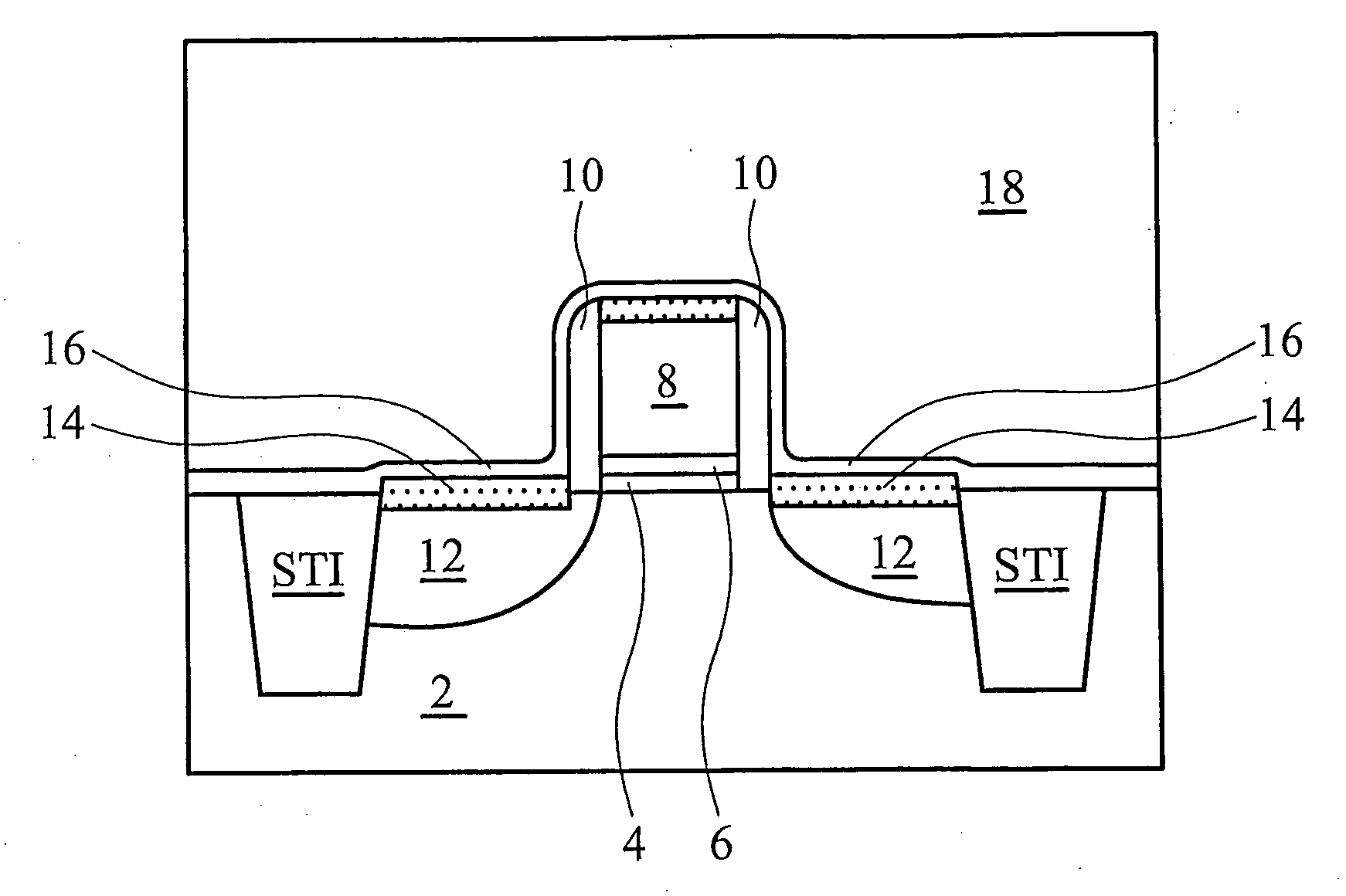
[0012]A novel metal-oxide-semiconductor (MOS) device having a stacked gate dielectric layer and methods for forming the same are provided by the present invention. The intermediate stages of manufacturing a preferred embodiment of the present invention are illustrated. Throughout the various views and illustrative embodiments of the present invention, like reference numbers are used to designate like elements.

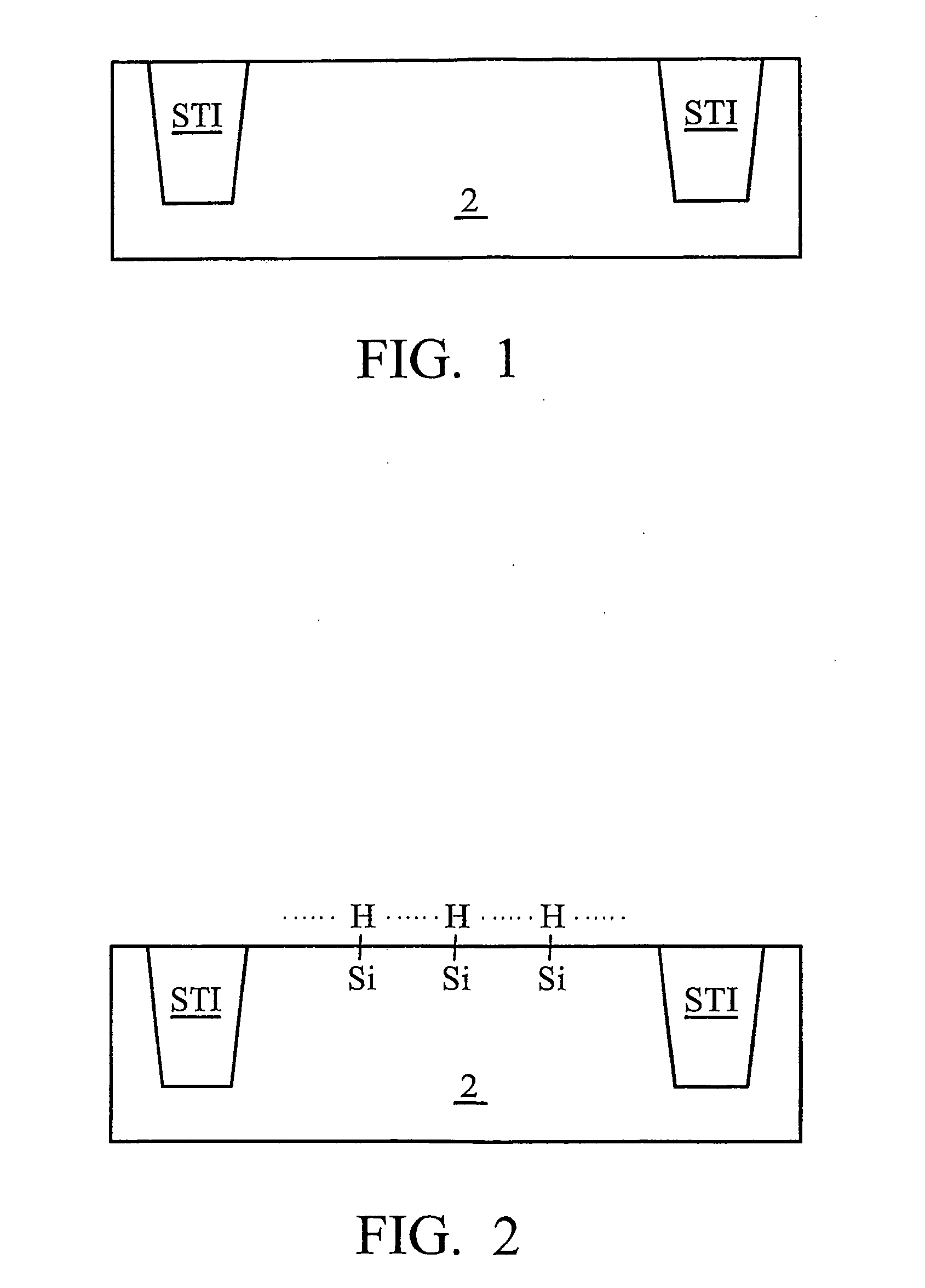
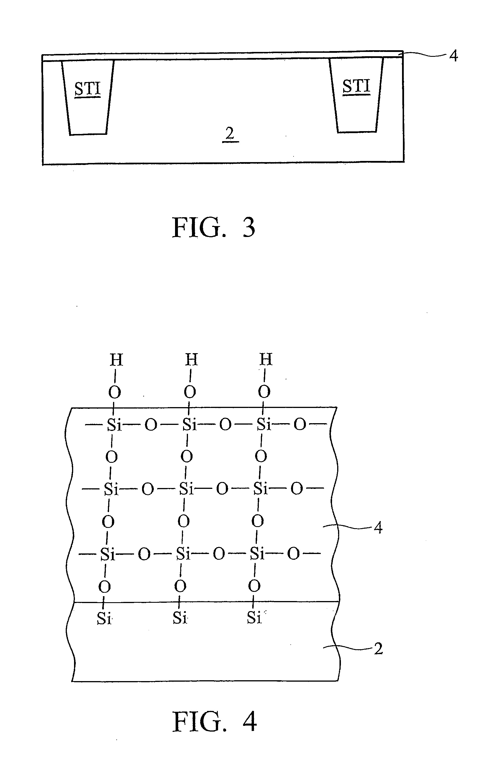
[0013]Referring to FIG. 1, a substrate 2, which is preferably a silicon substrate, is provided. Substrate 2 may also comprise other silicon-containing semiconductor mate...


PUM


Abstract

A method of forming a semiconductor structure includes providing a semiconductor substrate, performing a hydrogen annealing to the semiconductor substrate, forming a base oxide layer after the step of hydrogen annealing, and forming a high-k dielectric layer on the base oxide layer.

Description

TECHNICAL FIELD[0001]This invention is related generally to semiconductor devices, and more particularly to the structure and manufacturing methods of metal-oxide-semiconductor (MOS) devices.BACKGROUND[0002]With the scaling of integrated circuits, applications require an increasingly faster speed. This puts a requirement on the metal-oxide-semiconductor (MOS) devices, demanding that the MOS devices switch faster. As is known in the art, to increase the speed of MOS devices, high dielectric constant values (k values) of the gate dielectrics are desired. Since conventional silicon oxide, which has a k value of about 3.9, cannot satisfy such a requirement, high-k dielectric materials, which include oxides, nitrides, and oxynitrides, are increasingly used.[0003]High-k dielectric materials, however, have high trap densities, and thus cannot be used close to the channel regions of the MOS devices. A stacked gate dielectric scheme has been introduced to accommodate the benefit of the high-...

Claims


Application Information

Patent Timeline
IPC IPC(8): H01L21/00
CPCH01L21/02046H01L21/28185H01L21/28194H01L21/28211H01L29/665H01L21/31641H01L29/513H01L29/517H01L21/3141H01L21/02238H01L21/02194H01L21/02312H01L21/0228H01L21/02181
Inventor HSU, PENG-FUYING, JINTAO, HUN-JAN
Owner TAIWAN SEMICON MFG CO LTD
Why Eureka
Try Eureka