Integrated circuit (IC) package stacking and IC packages formed by same

a technology of integrated circuits and ic packages, applied in the direction of electrical equipment, semiconductor devices, semiconductor/solid-state device details, etc., can solve the problems of large package sizes, inconvenient mobile application, and inability to meet the requirements of mobile applications,

Active Publication Date: 2007-12-20
AVAGO TECH INT SALES PTE LTD
View PDF38 Cites 314 Cited by
  • Summary
  • Abstract
  • Description
  • Claims
  • Application Information

AI Technical Summary

Benefits of technology

[0055]Example embodiments of the present invention are described in detail below.
[0024]FIG. 1 illustrates a conventional plastic ball grid array (PBGA) integrated circuit (IC) package.
[0025]FIGS. 2A-2B illustrate views of the PBGA IC package of FIG. 1.
[0026]FIGS. 3A-3B illustrate views of a conventional fine pitch ball grid array (FBGA) IC package.
[0043]PBGA and FBGA packages are examples of conventional IC packages. Package on package (PoP) stacked IC packages referred to “as package stackable very-thin fine-pitch Ball Grid Array” (PSvfBGA) packages exist. See Dreiza et al, “Implement Stacked Package-on-Package Designs,” at http: / / www.eetasia.com / ARTICLES / 2005OCT / B / 2005OCT17_EDA_MFG_A.pdf) (hereinafter “Dreiza”), which is incorporated by reference herein in its entirety. FIGS. 4A-4B show examples of stacked PSvfBGA packages. FIG. 4A shows a stacked IC package 400. As shown in FIG. 4A, stacked IC package 400 includes a package-to-package interconnection made by mounting a top BGA package 430 to a substrate 410 of a bottom BGA package 440. Top and bottom BGA packages 430 and 440 are very fine-pitch BGA packages.
[0028]FIGS. 5A-5D illustrate views of example FBGA IC packages having interconnect members, according to exemplary embodiments of the invention.
[0061]FIGS. 6A-6C illustrate example IC packages, according to embodiments of the present invention. FIG. 6A shows a package 600 in which interconnect members 508 are attached to a top surface of die 102. Encapsulating material 512 encapsulates the top surface of substrate 110, die 102, and wirebonds 114. Furthermore, interconnect members 508 are fully encapsulated by encapsulating material 512. FIG. 6B illustrates an example package 650, where a top layer of encapsulating material 512 has been removed and interconnect members 508 have been thereby truncated. Surfaces (interconnect contact pads) 504 are formed on the top surface of encapsulating material 512.
[0065]FIGS. 7A-7D illustrate example embodiments of stacked FBGA packages. FIG. 7A illustrates a stacked IC package 700 that includes a second IC package 740 mounted on a first IC package 730. Second package 730 is configured similarly to package 300 shown in FIG. 3B. First package 740 is configured similarly to package 650 of FIG. 6B. Solder balls 108 on a bottom surface of substrate 110 of second package 730 are electrically coupled a plurality of interconnect members 508 accessible at a top surface 702 of encapsulating material 112 of first IC package 740. In particular, solder balls 108 are attached to surfaces 504 of interconnect members 508.
[0031]FIGS. 8A-8B illustrate cross-sectional views of example PoP stacked IC packages, according to exemplary embodiments of the invention.
[0032]FIGS. 9A and 9B illustrates cross-sectional views of example PoP stacked IC packages, according to exemplary embodiments of the invention.
[0033]FIG. 10 illustrates an example flowchart for manufacturing IC packages, according to exemplary embodiments of the invention.
[0034]FIGS. 11A-11H illustrate cross-sectional views of example IC packages at various stages of manufacture, according to exemplary embodiments of the invention.

Problems solved by technology

Therefore, the size of the IC die is limited by the size of the mold cap (i.e., the mold cavity).
Large package sizes are undesirable for mobile applications where bulky electronic components make for bulky devices.
However, while providing some improvement, FBGA packages still suffer from the disadvantages described above with regard to PBGA packages.

Method used


Image

  • Integrated circuit (IC) package stacking and IC packages formed by same
  • Integrated circuit (IC) package stacking and IC packages formed by same
  • Integrated circuit (IC) package stacking and IC packages formed by same

Examples


Embodiment Construction

Introduction

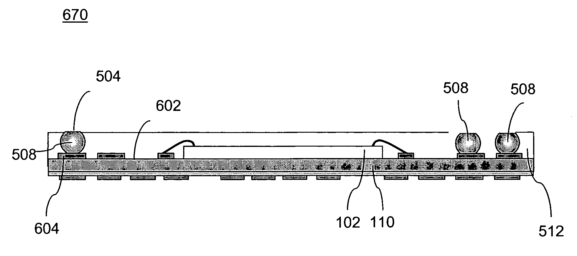
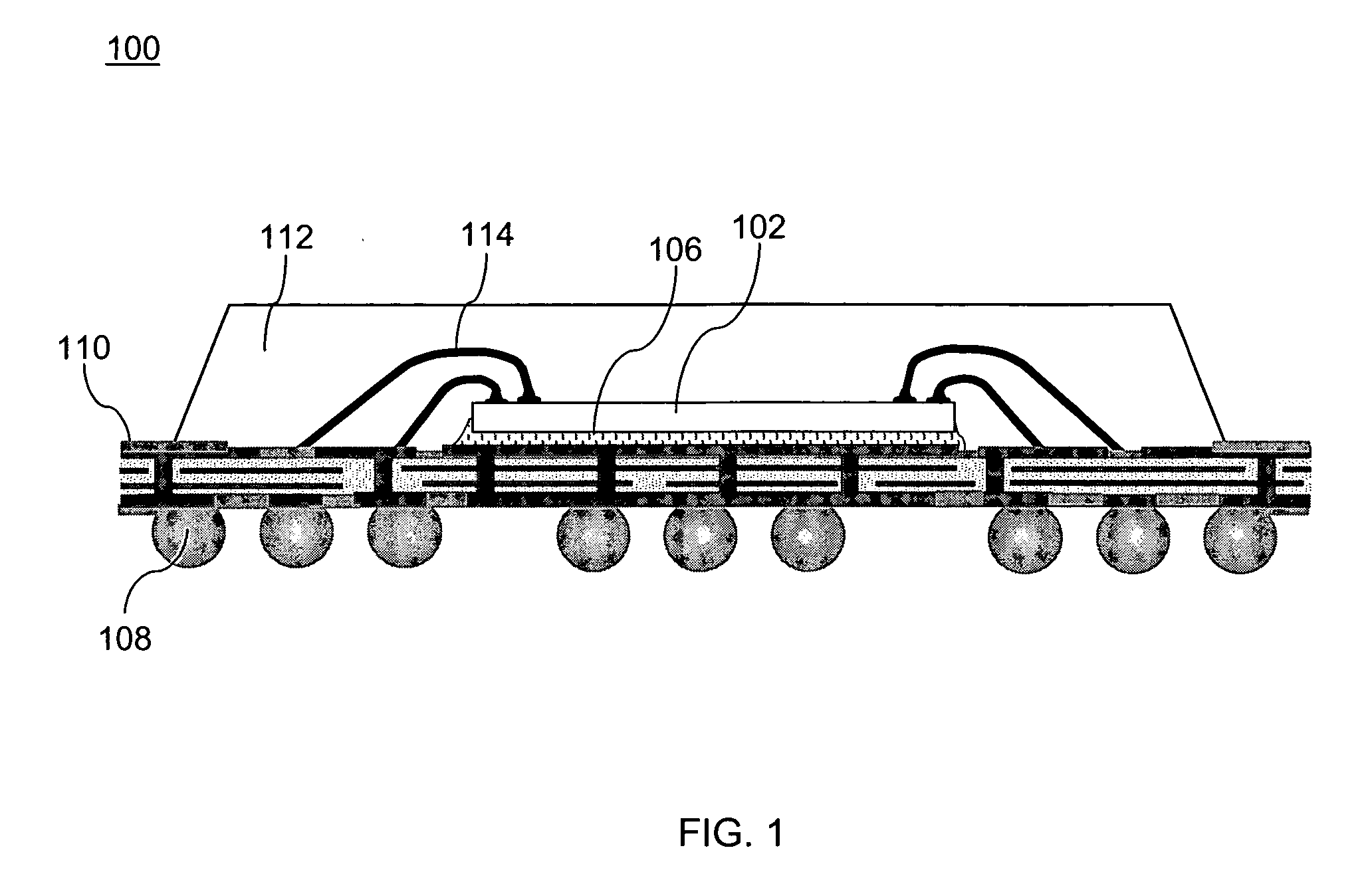
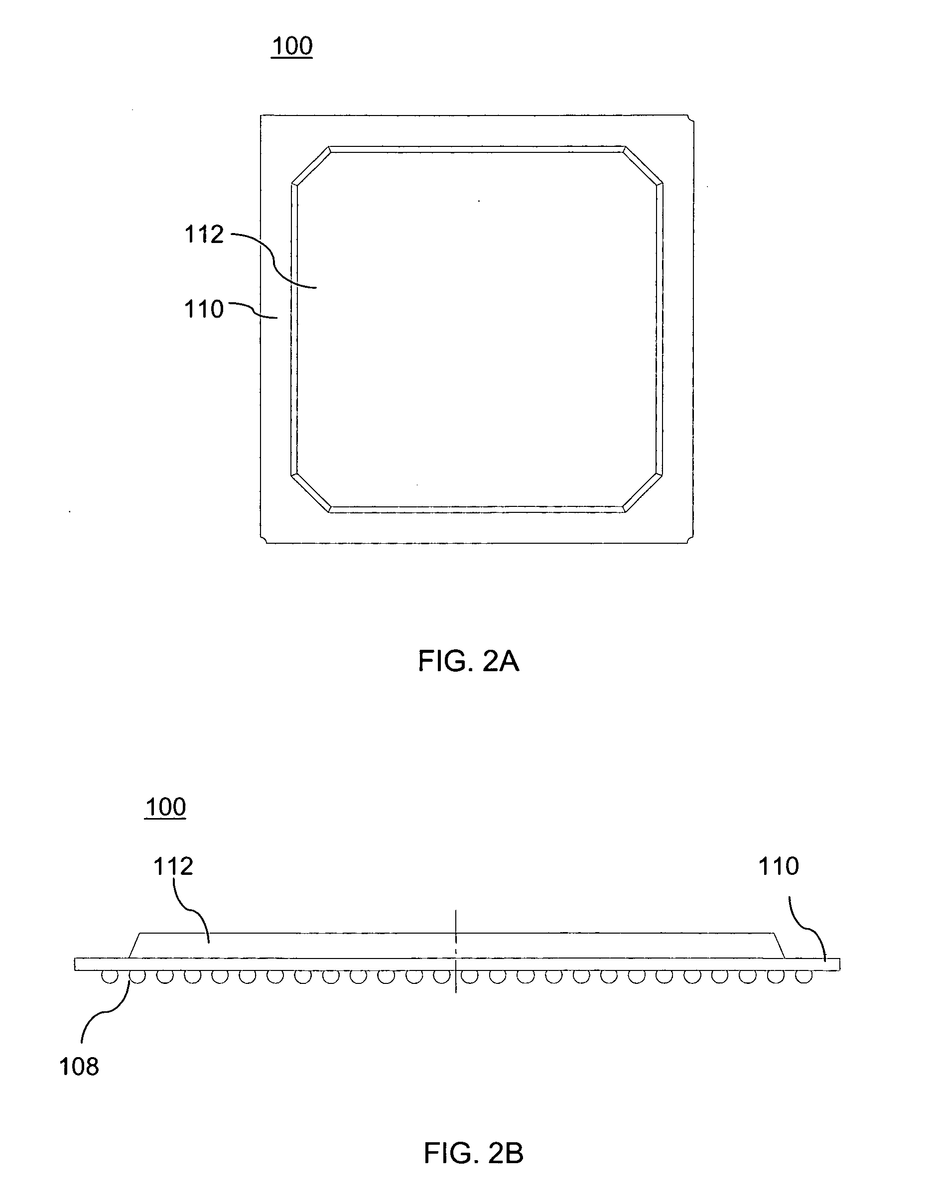
[0037]Methods, systems, and apparatuses for IC device packaging technology are described herein. In particular, methods, systems, and apparatuses for package to package interconnection of IC packages to form improved IC packages are described.

[0038]References in the specification to “one embodiment,”“an embodiment,”“an example embodiment,” etc., indicate that the embodiment described may include a particular feature, structure, or characteristic, but every embodiment may not necessarily include the particular feature, structure, or characteristic. Moreover, such phrases are not necessarily referring to the same embodiment. Further, when a particular feature, structure, or characteristic is described in connection with an embodiment, it is submitted that it is within the knowledge of one skilled in the art to effect such feature, structure, or characteristic in connection with other embodiments whether or not explicitly described.

[0039]The present specification discloses ...


PUM


Abstract

Methods, systems, and apparatuses for integrated circuit (IC) package vertical interconnection are described herein. In an aspect of the invention, an IC package includes an IC die with contact pads. The IC package also includes interconnect members which are coupled to the die at the contact pads. An encapsulating material encapsulates the IC die and the interconnect members such that a contact surface of each interconnect member is accessible at a surface of the encapsulating material. A second IC package is coupled to the first IC package through the plurality of interconnect members of the first IC package. In an example, solder balls attached to a bottom of the second IC package are coupled to the contact surfaces of the interconnect members to couple the first IC package and the second IC package.

Description

[0001]This application claims the benefit of U.S. Provisional Appl. No. 60 / 814,875, filed Jun. 20, 2006, which is herein incorporated by reference in its entirety.BACKGROUND OF THE INVENTION[0002]1. Field of the Invention[0003]The invention relates generally to the field of integrated circuit (IC) device packaging technology, and more particularly to package to package interconnection of IC packages.[0004]2. Background Art[0005]The die-up plastic ball grid array package (PBGA) was first introduced by Motorola and was called an overmolded plastic pad array carriers (OMPAC). See Freyman, and Pennisi, “Overmolded Plastic Pad Array Carriers (OMPAC): A Low Cost, High Interconnect Density IC Packaging Solution for Consumer and Industrial Electronics,” Electronic Components and Technology Conference, IEEE, pp. 176-182, (1991), which is incorporated by reference herein in its entirety.[0006]A PBGA package features a plastic printed circuit board (substrate) typically made of BT (Bismaleimid...

Claims


Application Information

Patent Timeline
Patent Type & Authority Applications(United States)
IPC IPC(8): H01L23/28
CPCH01L2924/15321H01L24/91H01L2924/01033H01L2924/01047H01L2224/92127H01L2924/15331H01L2225/1088H01L2924/01079H01L2224/73207H01L2924/01027H01L2224/48091H01L2924/01005H01L25/105H01L2225/1058H01L24/73H01L2924/01006H01L21/56H01L2924/014H01L2924/19043H01L2924/19041H01L24/13H01L2224/48227H01L2924/15311H01L2224/32145H01L2924/14H01L2924/3011H01L2924/19042H01L2224/48465H01L24/10H01L2225/1023H01L2924/01082H01L23/3128H01L2224/73265H01L2225/06568H01L2924/01029H01L24/48H01L2224/92242H01L2224/32225H01L2224/13099H01L2924/01013H01L2924/1815H01L2924/00014H01L2924/00012H01L2924/00H01L2224/13H01L2224/48237H01L2924/12042H01L2924/181H01L2224/45099H01L2224/45015H01L2924/207H01L23/02H01L23/12H01L23/28
Inventor ZHAO, SAM ZIQUNKHAN, REZAUR RAHMAN
Owner AVAGO TECH INT SALES PTE LTD
Why Eureka
Try Eureka