Probe card

Inactive Publication Date: 2007-12-20
TOKYO ELECTRON LTD
View PDF9 Cites 15 Cited by
  • Summary
  • Abstract
  • Description
  • Claims
  • Application Information

AI Technical Summary

Benefits of technology

[0021]According to the present invention, a probe card that can correspond to an examinati

Problems solved by technology

However, in the above probe card, manufacturing has been taking time because it is necessary to form very complicated and fine wiring.
Also

Method used


Image

  • Probe card
  • Probe card
  • Probe card

Examples


Embodiment Construction

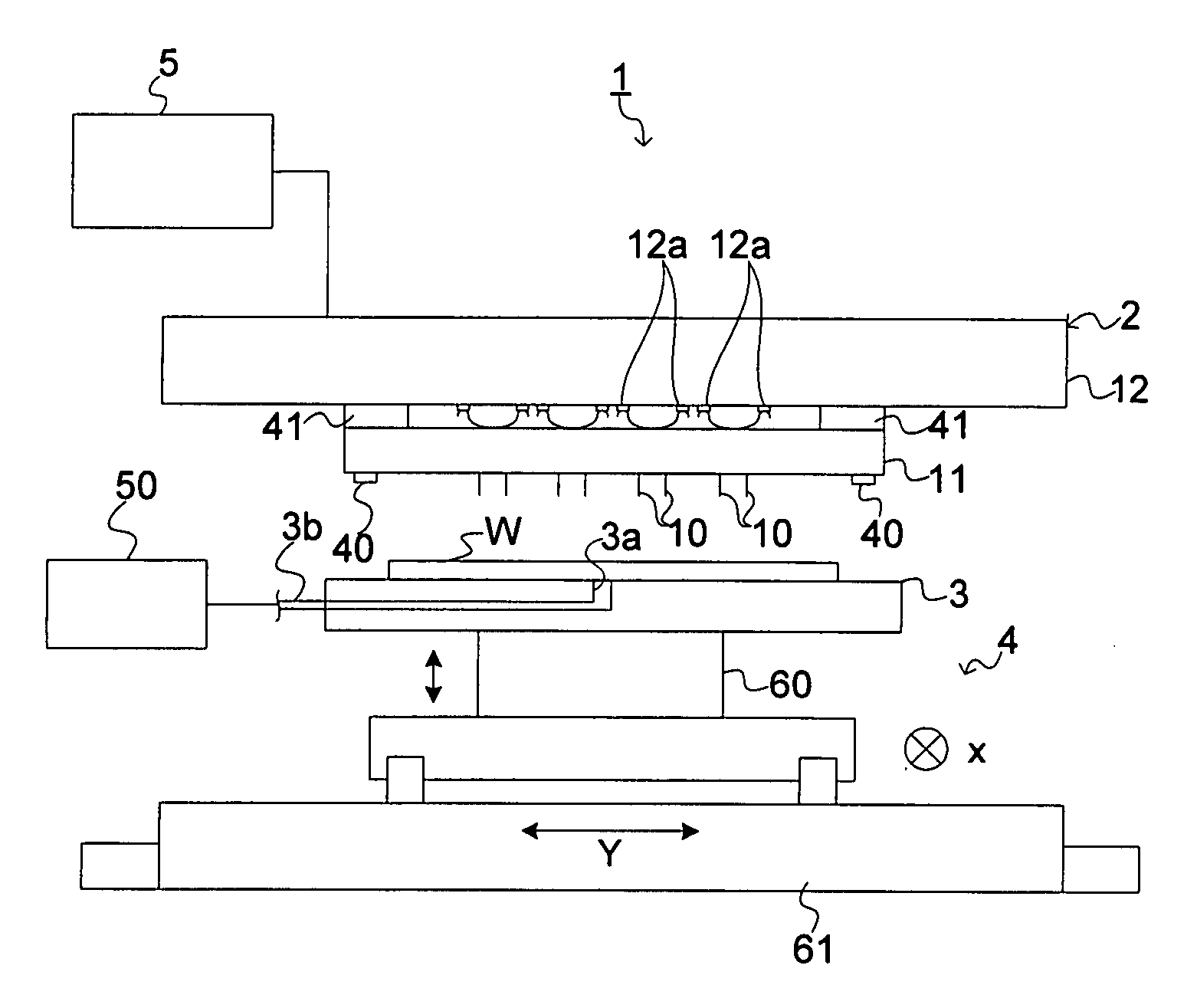
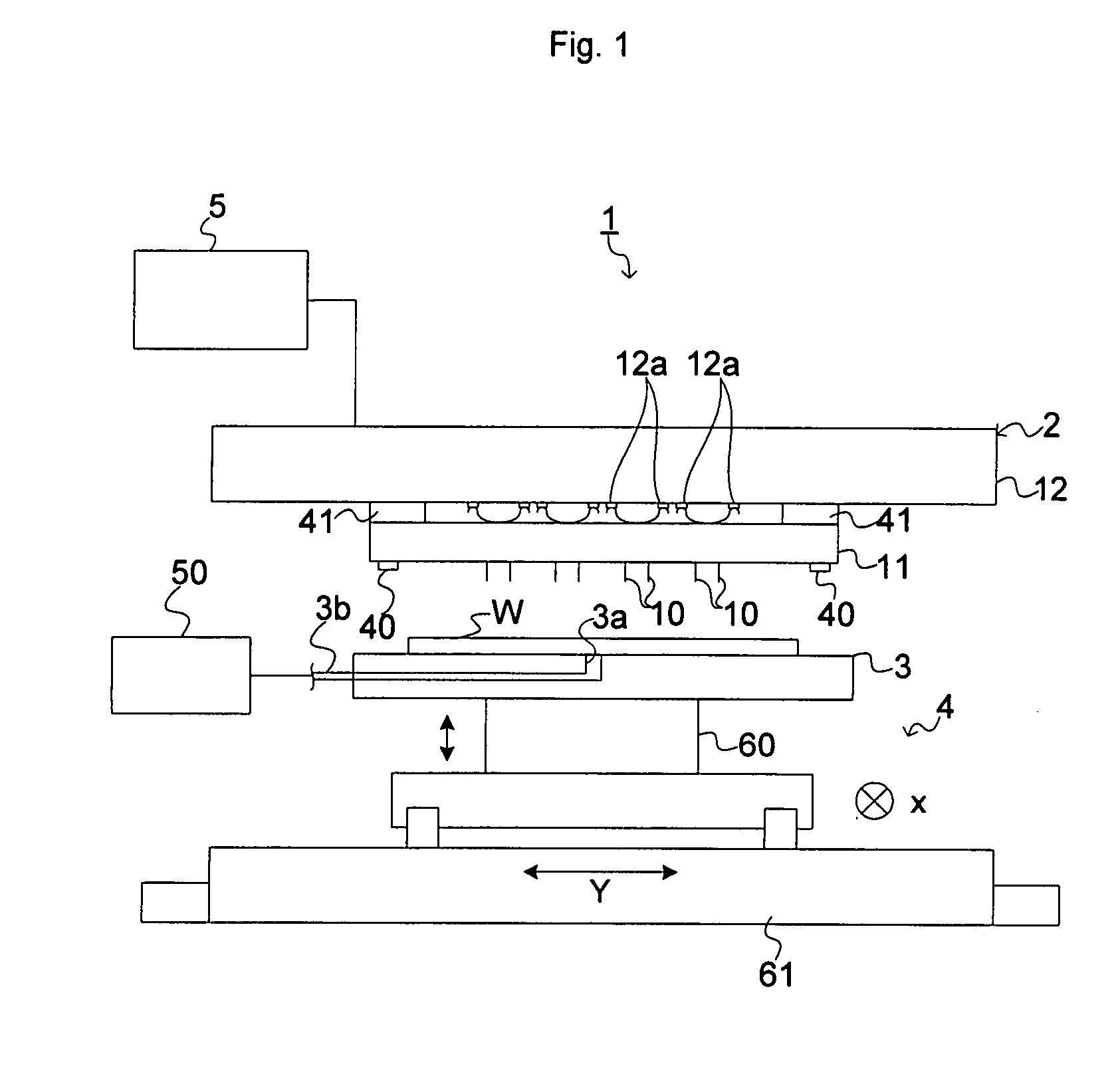
[0041]A preferred embodiment of the present invention will hereinafter be described. FIG. 1 is an explanatory diagram showing a configuration of a probe 1 having a probe card according to the embodiment.

[0042]The probe 1 is provided with, for example, a probe card 2, a chuck 3 to stick and retain a wafer W, as an examination object, a moving mechanism 4 for moving the chuck 3, and a tester 5.

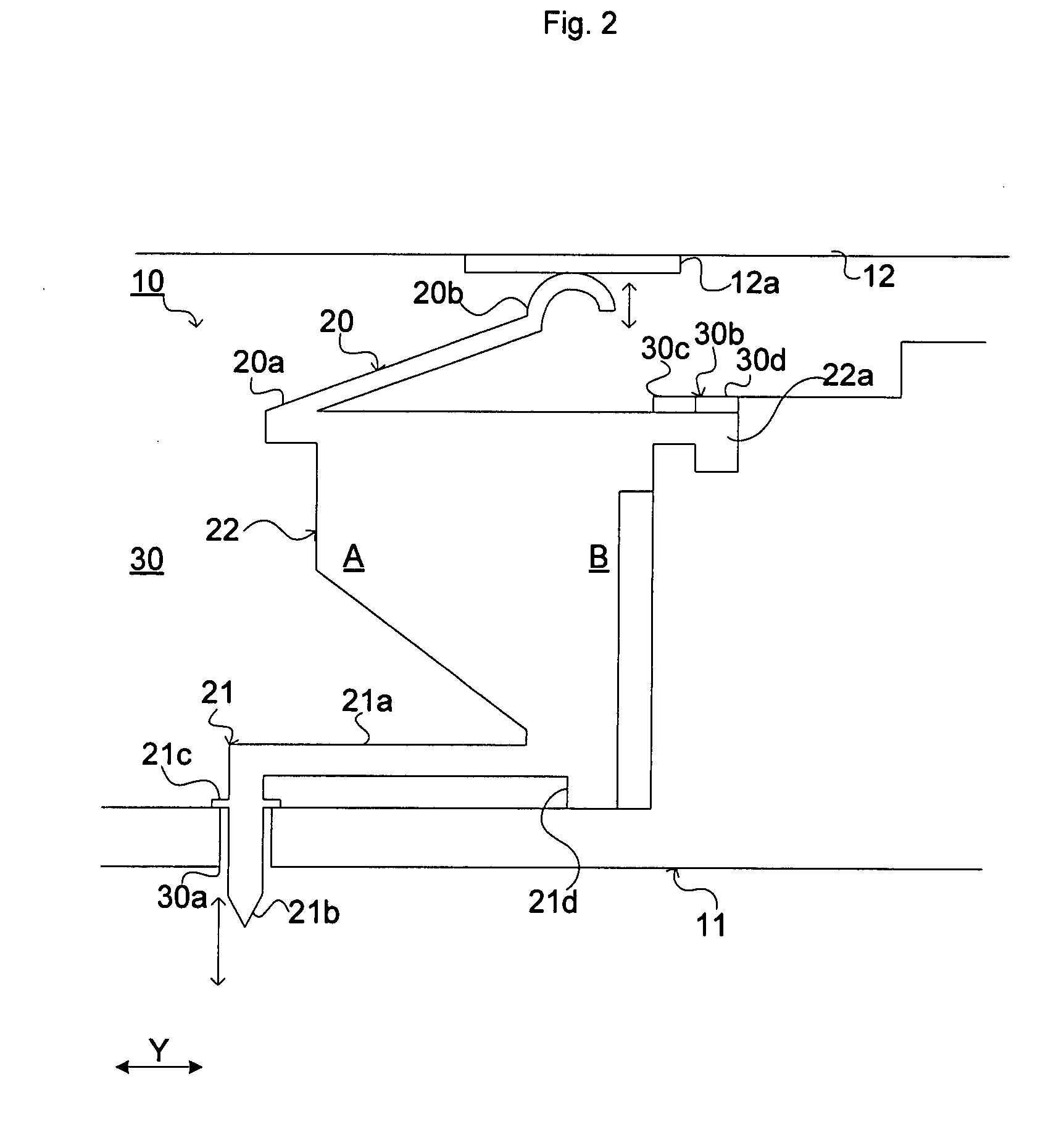
[0043]The probe card 2 is provided with, for example, a plurality of probes 10, a probe supporting plate 11 which supports the probe 10 while the probes 10 are inserted, and a printed wiring board 12 as a circuit board, attached on the upper face side of the probe supporting plate 11.

[0044]The printed wiring board 12 is electrically connected to the tester 5. Inside of the printed wiring board 12, a wiring for an electrical signal for examination to travel from the tester 5 is formed, and a plurality of terminals 12a for the wiring are formed on a lower face of the printed wiring board 12.

[0045]...


PUM

PropertyMeasurementUnit
Shapeaaaaaaaaaa
Distanceaaaaaaaaaa

Abstract

The present invention provides a probe card that can examine an object with small electrode spacing. A probe supporting plate is provided to a lower face side of a printed wiring board of a probe card. A plurality of probes are supported by the probe supporting plate. The probes comprise an upper contact, a lower contact, and a main body portion. An upper end portion of the upper contact protrudes toward an upper side of the probe supporting plate and contacts a terminal of the printed wiring board. A lower end portion of the lower contact protrudes toward a lower side of the probe supporting plate. On the probe supporting plate, a through-hole and a concave portion are formed to lock the probes, and the probes can be inserted and removed freely against the probe supporting plate from above.

Description

TECHNICAL FIELD[0001]The present invention relates to a probe card for examining electrical characteristics of an examination object, such as a wafer.BACKGROUND OF INVENTION[0002]Examinations of electrical characteristics of an electronic circuit, such as an IC or an LSI formed on a semiconductor wafer, have been typically carried out by the use of examination devices having a probe card. The probe card typically comprises plurality of probe pins to be contacted to a large number of electrodes on a wafer, and a circuit board transmits an electric signal to each probe for examination. The examination of the electric circuit on the wafer has been carried out in such way that each electrode of the wafer are brought into contact with each probe pin, and an electrical signal is transmitted from the circuit board to each probe.[0003]In recent years, spacing between electrodes of an electronic circuit on a wafer are getting smaller, and are now down to approximately tens of μm to 100 μm du...

Claims


Application Information

Patent Timeline
IPC IPC(8): G01R1/067
CPCG01R1/06733G01R1/07371Y10T29/49204H01L2924/00013H01L2224/29099G01R1/067
Inventor MOCHIZUKI, JUNHOSAKA, HISATOMI
Owner TOKYO ELECTRON LTD
Why Eureka
Try Eureka