
Display substrate having integrated bypass capacitors, display device having the same and method of manufacturing the same

a technology of bypass capacitors and display substrates, applied in the direction of optics, electric digital data processing, instruments, etc., can solve the problems of unstable data signal output from difficult formation of bypass capacitors for stabilizing the output signal of the source driving circuit, and poor display quality

Inactive Publication Date: 2007-12-20
SAMSUNG ELECTRONICS CO LTD
View PDF0 Cites 14 Cited by
  • Summary
  • Abstract
  • Description
  • Claims
  • Application Information

AI Technical Summary

Benefits of technology

The present invention provides a way to improve the reliability of panel driving data signals by adding one or more bypass capacitors on the display panel. This helps to stabilize the data signal and remove ripple components, resulting in better display quality. The invention involves integrating a conductive pattern with the power wiring section of the panel to create a shunting path for AC voltage signals. This helps to stabilize the data signal and remove ripple components, resulting in better display quality.

Problems solved by technology

However, when the COG method is employed, formation of the bypass capacitor for stabilizing the output signal of the source driving circuit is not easy, especially if it is to be formed integrally on the same dielectric substrate adjacent to its corresponding output buffer.
Consequently, those who have heretofore employed the COG method have shied away from having an adjacent bypass capacitor and the data signal output from the source driving circuit has had a tendency to be unstable due to insufficient damping of the ripple component by the missing bypass capacitor, and as a result, display quality has suffered when the COG method is adopted.

Method used


Image

  • Display substrate having integrated bypass capacitors, display device having the same and method of manufacturing the same
  • Display substrate having integrated bypass capacitors, display device having the same and method of manufacturing the same
  • Display substrate having integrated bypass capacitors, display device having the same and method of manufacturing the same

Examples


Embodiment Construction

[0022]It is to be understood that when an element or layer is referred to herein as being “on,”“connected to” or “coupled to” another element or layer, it can be either directly on, connected to or coupled to the other element or layer, or one or more intervening elements or layers may be present for providing indirect coupling. In contrast, when an element is referred to herein as being “directly on,”“directly connected to” or “directly coupled to” the other element or layer, there are no intervening elements or layers present. Like numbers refer to like elements throughout. As used herein, the term “and / or” includes any and all combinations of one or more of the associated listed items.

[0023]It will be understood that, although the terms first, second, third etc. may be used herein to describe various elements, components, regions, layers and / or sections, these elements, components, regions, layers and / or sections should not be limited in number by these terms. These terms are onl...


PUM


Abstract

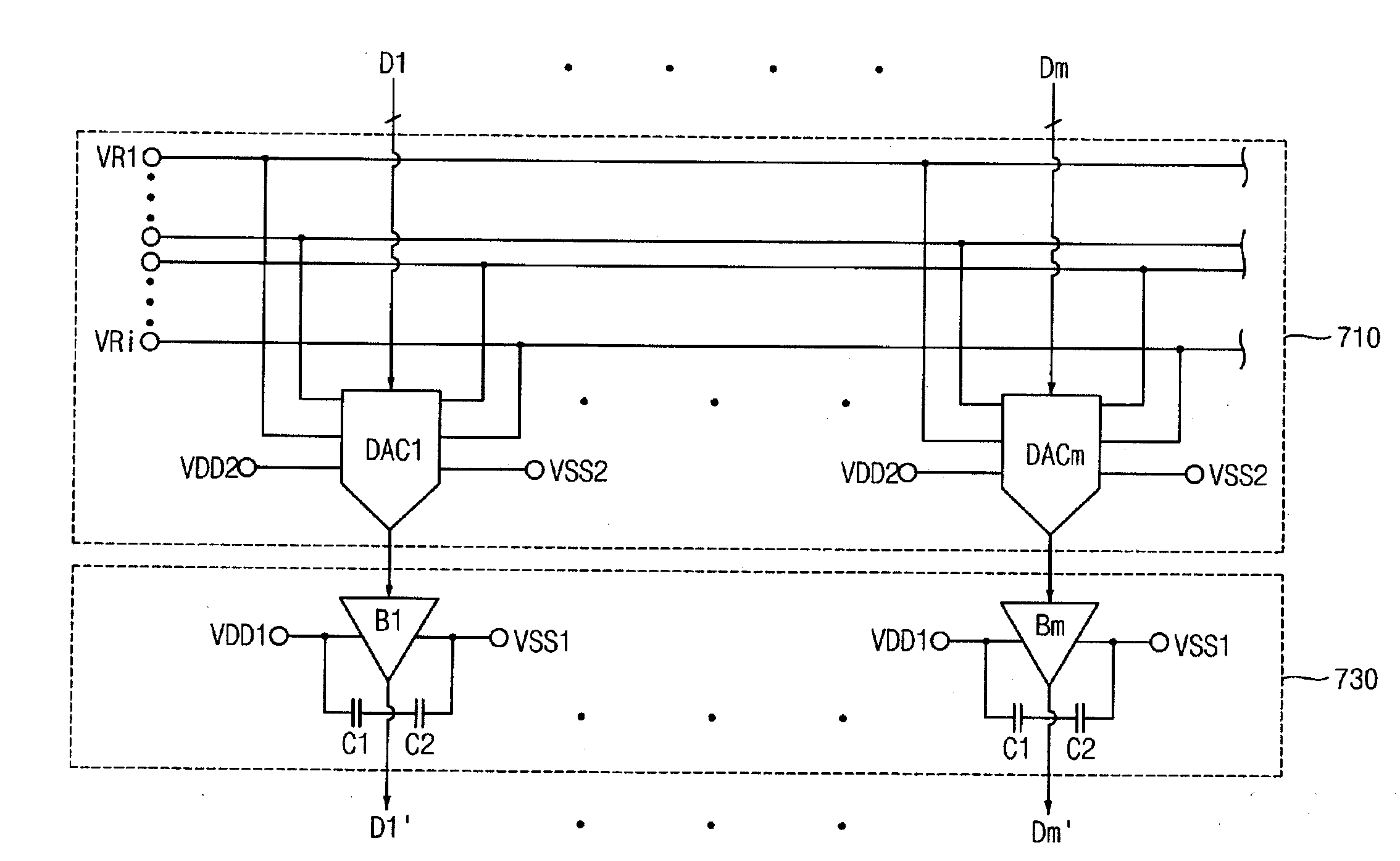
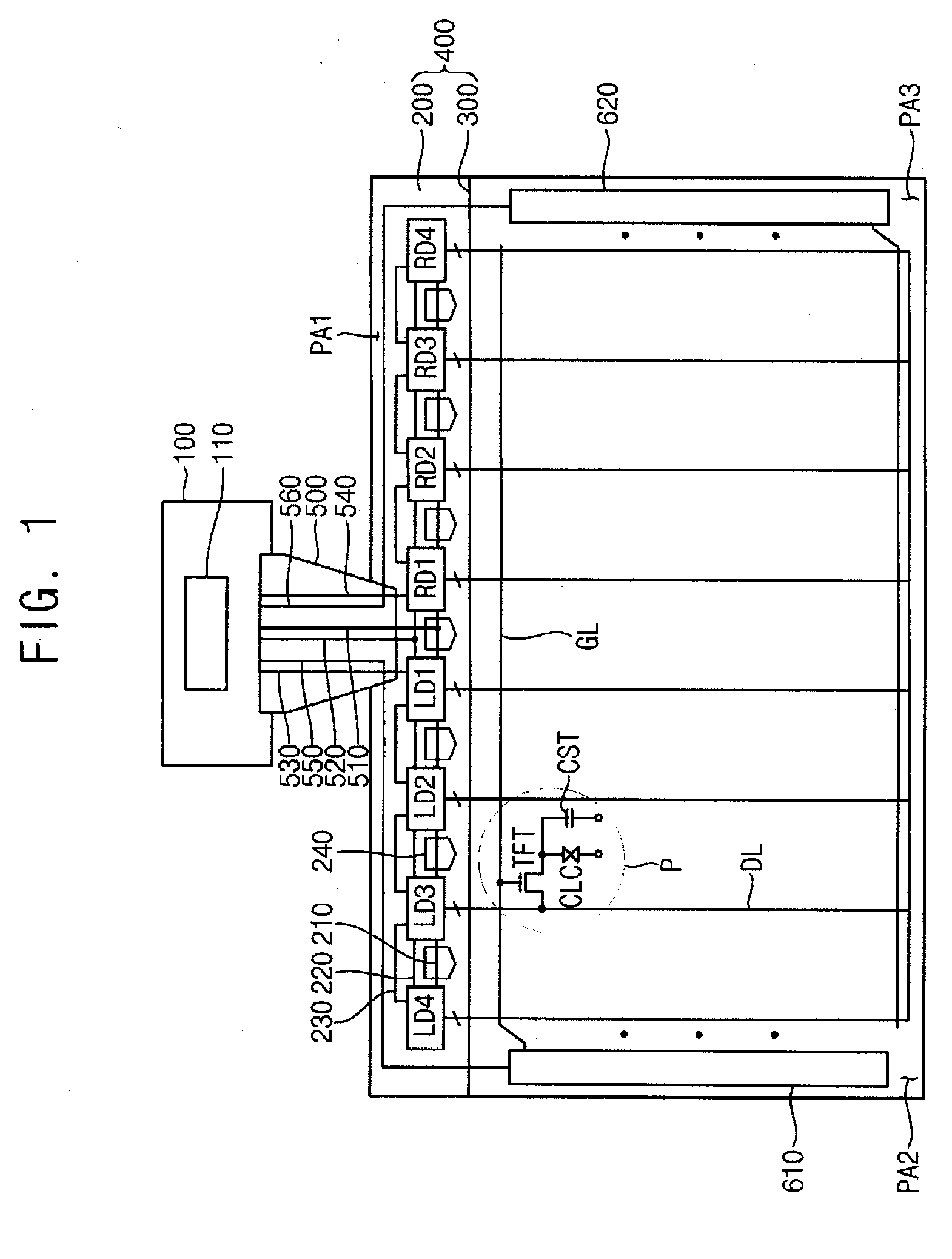
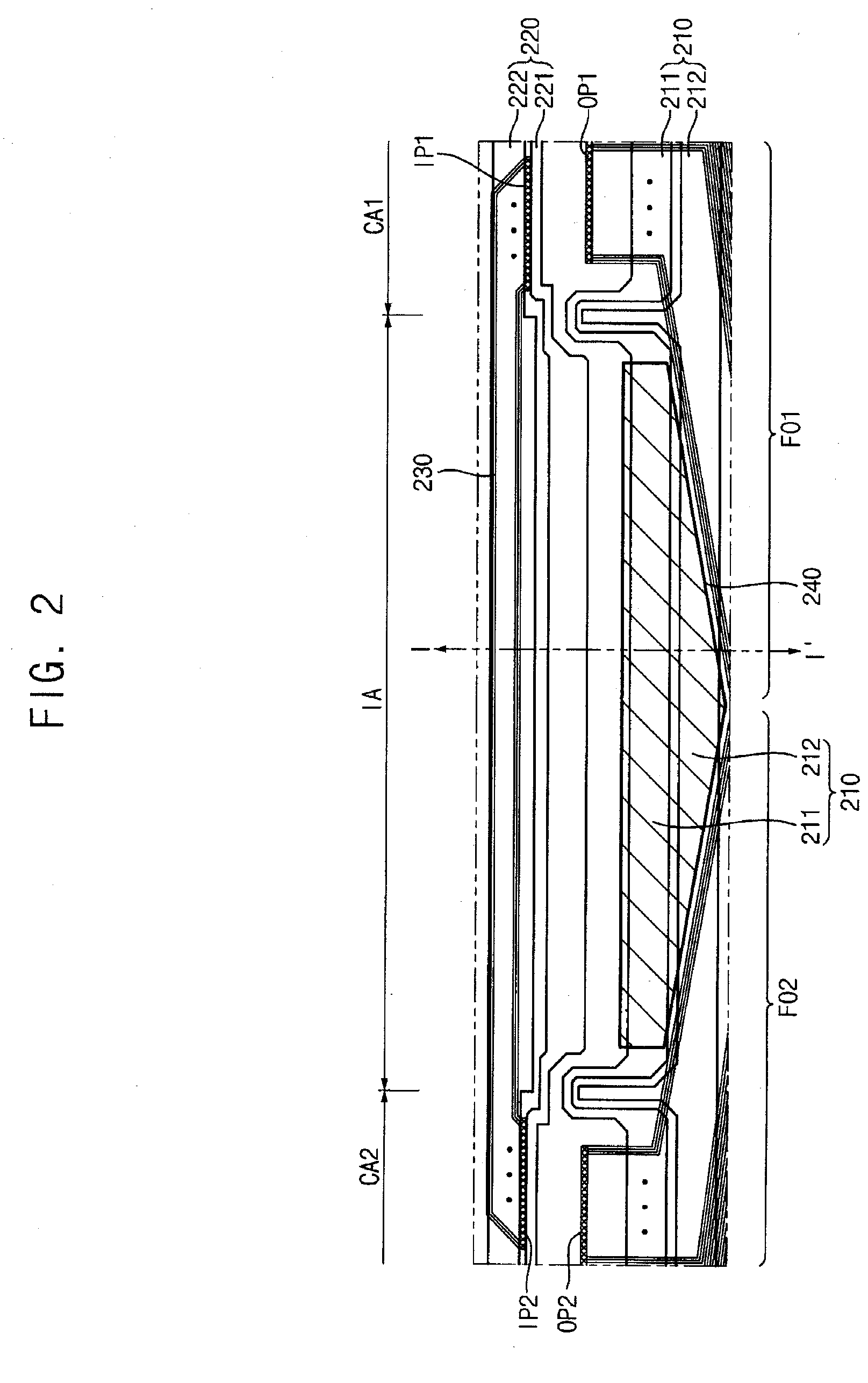
A display substrate includes an output pads section, a fan-out section, a first power wiring section and a first conductive pattern. The output pads section is electrically connected to a plurality of output terminals of a first driver chip. The fan-out section electrically connects the output pads section to a plurality of source wirings. The first power wiring section is extended along a longitudinal direction of a plurality of gate wirings that cross with source wirings of the display substrate. The first power wiring section propagates at least first and second power-delivering voltages to the driver chip. The first conductive pattern is insulatively overlapped with the first power wiring section in an intermediate area between the output pads sections of an adjacent second driver chip. The first conductive pattern thereby defines a capacitive shunting path for voltage transients or ripples.

Description

CROSS-REFERENCE TO RELATED APPLICATIONS[0001]This application claims priority under 35 U.S.C. §119 to Korean Patent Application No. 2006-54699 filed on Jun. 19, 2006 in the Korean Intellectual Property Office (KIPO), the disclosure of which is herein incorporated by reference.BACKGROUND[0002]1. Field of Invention[0003]The present disclosure of invention relates to on-glass or on-substrate integrated circuitry such as found in Liquid Crystal Display (LCD) devices and more particularly to a transparent display substrate comprising a means for enhancing reliable switching of a driving signal that is generated by an on-substrate circuit, and a display device having the reliability-enhanced display substrate.[0004]2. Description of Related Art[0005]Generally, a liquid crystal display (LCD) device includes a display panel that displays an image using light transmittance through a liquid crystal material and through a transparent substrate such as one made of glass, where the panel include...

Claims


Application Information

Patent Timeline
Patent Type & Authority Applications(United States)
IPC IPC(8): G06F13/18
CPCG02F1/1345G02F1/13452G09G2310/027G09G2300/0408G09G3/3688
Inventor KWAK, YUN-HEECHANG, JONG-WOONGMOON, SEUNG-HWAN
Owner SAMSUNG ELECTRONICS CO LTD
Learn More