
Compact and miniature optical navigation device

a technology of optical navigation and compact structure, applied in the direction of color television details, television systems, instruments, etc., can solve the problems of inability to apply to a small form factor product or a device having multiple chips, difficult assembly, and high cost of optical navigation devices, etc., to achieve the effect of convenient surface mounting

Inactive Publication Date: 2007-12-20
HARVATEK CORPORATION
View PDF7 Cites 23 Cited by
  • Summary
  • Abstract
  • Description
  • Claims
  • Application Information

AI Technical Summary

Benefits of technology

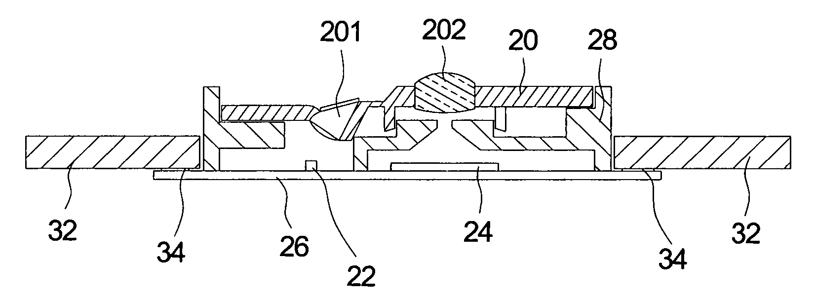
[0008]One particular aspect of the present invention is to provide a compact and miniature optical navigation device. The compact and miniature optical navigation device is packaged at a system level with multiple chips, including a source (such as a light source) and a detector etc, for providing the required optical illumination channel and imaging channel. The entire system is packaged in a small form factor such that its assembly can be applied in various small form outlines with the ease of surface mounting capabilities.
[0009]Another particular aspect of the present invention is to provide a compact and miniature optical navigation device. The compact and miniature optical navigation device can be used in various applications ranging from a hand held navigation tool suitable for application in cell phones to that of computer or lap top navigation devices. With the application in cell phones, this gives the user the mobility of moving the curser 360 degrees around the display.
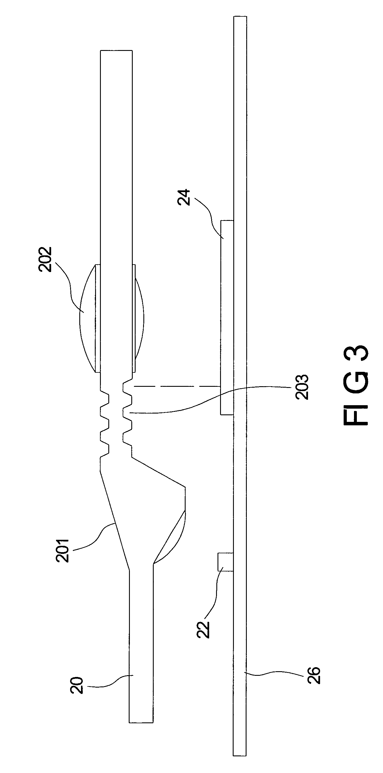
[0010]A further particular aspect of the present invention is to provide a compact and miniature optical navigation device. The compact and miniature optical navigation device integrates the illumination channel and the imaging channel into one piece to achieve the effects of miniaturizing the device and simplifying the manufacturing process. The novelty of the present invention is the integration of the optical system, mechanical structure and electronic system into a small form factor package.
[0011]In another preferred embodiment, the navigation device consists of one single piece part which integrates the imaging and illumination channel with an opening through hole in between the imaging channel and illumination channel. One completion of the assembly of this package, the module will be surface mounted on the customer's board. In order to reduce the total height of the module, a through hole that fits the outline of the package is drilled or punched. Surface mounting pads which match a similar surface mounting pad on the substrate of the package is then interconnected through a conductive material typically solder. Having this feature allows the overall package height to be reduced depending on the customer board thickness.

Problems solved by technology

However, the light source and the sensor of the optical navigation device are independent and they are not located on a common platform during assembly.
Therefore, the assembly is difficult and the cost of the optical navigation device is expensive.
Therefore, it cannot be applied to a small form factor product or a device having multiple chips.
During the assembling process, mechanical alignment of the optical navigation device is more complex and difficult.

Method used


Image

  • Compact and miniature optical navigation device
  • Compact and miniature optical navigation device
  • Compact and miniature optical navigation device

Examples


Embodiment Construction

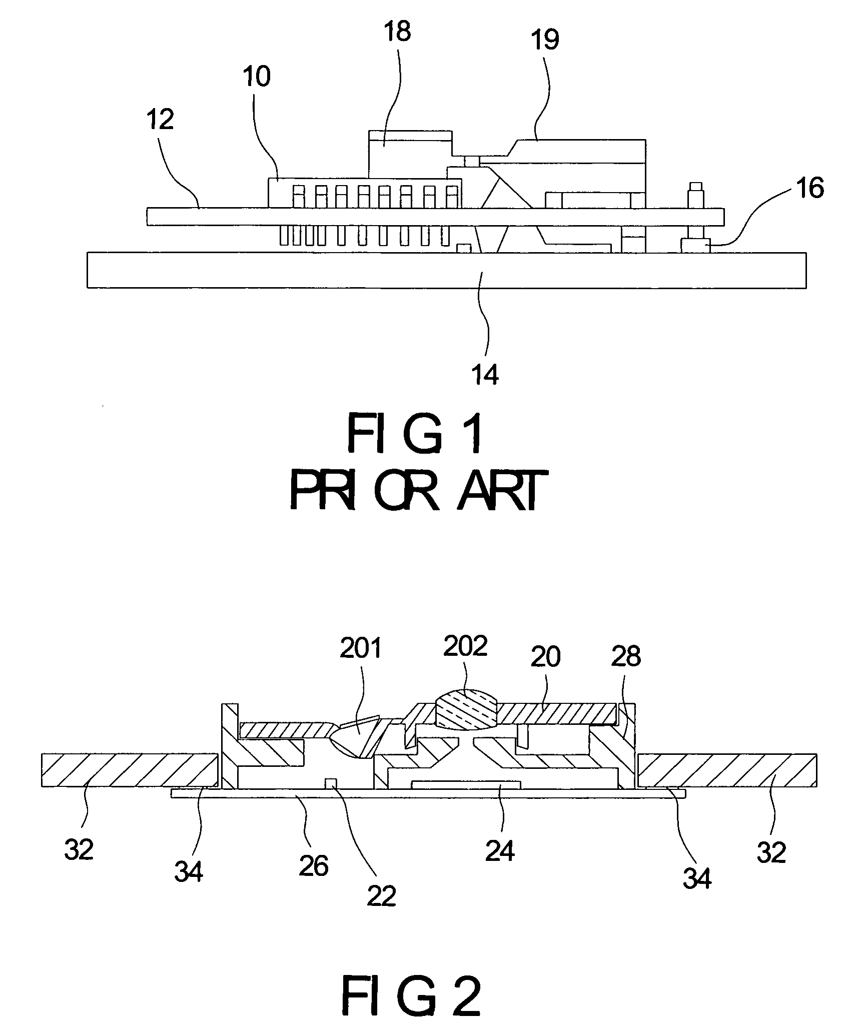
[0021]Please refer to FIG. 1, which shows a schematic diagram of the compact and miniature optical navigation device of the present invention. The present invention is an overall compact solution of all optical, mechanical and electrical systems integrated into a small size. Its size is greatly reduced compared to the prior art. In the present invention, the illumination channel 201 and the imaging channel 202 are integrated into one piece. This is achieved by various known molding technologies, such as the photo-imaging element shown in the FIG. 2 to achieve the effect of simplifying the manufacturing process. When the light is emitted from the light source 22, the light passes through the illumination channel 201 and arrives at the surface that the compact and miniature optical navigation device is navigating. Then, the light is reflected from the surface, passes through the imaging channel 202, and is received by a sensor 24. Thereby, the location that the compact and miniature o...


PUM


Abstract

A compact and miniature optical navigation device integrates an illumination channel and an imaging channel into single piece. The present invention integrates the optical system, the mechanical system, and the electrical system into a small form factor device. The compact and miniature optical navigation device includes a photo-imaging element, a housing, and a first substrate. The photo-imaging element comprises an imaging channel and an illumination channel. The housing includes an aperture stop and an alignment element. The aperture stop and the housing are integrated into one piece and the alignment element is part of the housing. The first substrate includes a light source and a sensor. The light source and the sensor are located on the same surface of the first substrate. The light emitted from the light source passes through the illumination channel, reflected from the navigating surface and forms the image on the sensor.

Description

BACKGROUND OF THE INVENTION[0001]1. Field of the Invention[0002]The present invention relates to a compact and miniature optical navigation device. In particular, the present invention relates to a compact and miniature optical navigation device that is composed of a light source and a sensor.[0003]2. Description of the Related Art[0004]An optical navigation device typically consists of an optical imaging sensor and an imaging processing chip used for recording images of a surface that the optical navigation device is navigating over. The sensor captures images of the surface and compares the subsequent image of the surface when the optical navigation device is navigating. The images are recorded at a very high rate. The sensor incorporates electronic circuitry to compute and determine where the optical navigation device moves in horizontal and vertical directions.[0005]FIG. 1 shows a schematic diagram of the optical navigation device of the prior art. The optical navigation sensor ...

Claims


Application Information

Patent Timeline
Patent Type & Authority Applications(United States)
IPC IPC(8): H04N5/222
CPCG06F3/0317
Inventor GOH, KEE-SIANGTAI, KEAN-LEONGBALWANT SINGH, GURBIR SINGH A/LWANG, BILY
Owner HARVATEK CORPORATION
Learn More