
Non-volatile memory device having four storage node films and methods of operating and manufacturing the same

a non-volatile memory and storage node technology, applied in semiconductor devices, digital storage, instruments, etc., can solve the problem of limited spacing between the fins

Inactive Publication Date: 2007-12-27
SAMSUNG ELECTRONICS CO LTD
View PDF3 Cites 19 Cited by
  • Summary
  • Abstract
  • Description
  • Claims
  • Application Information

AI Technical Summary

Benefits of technology

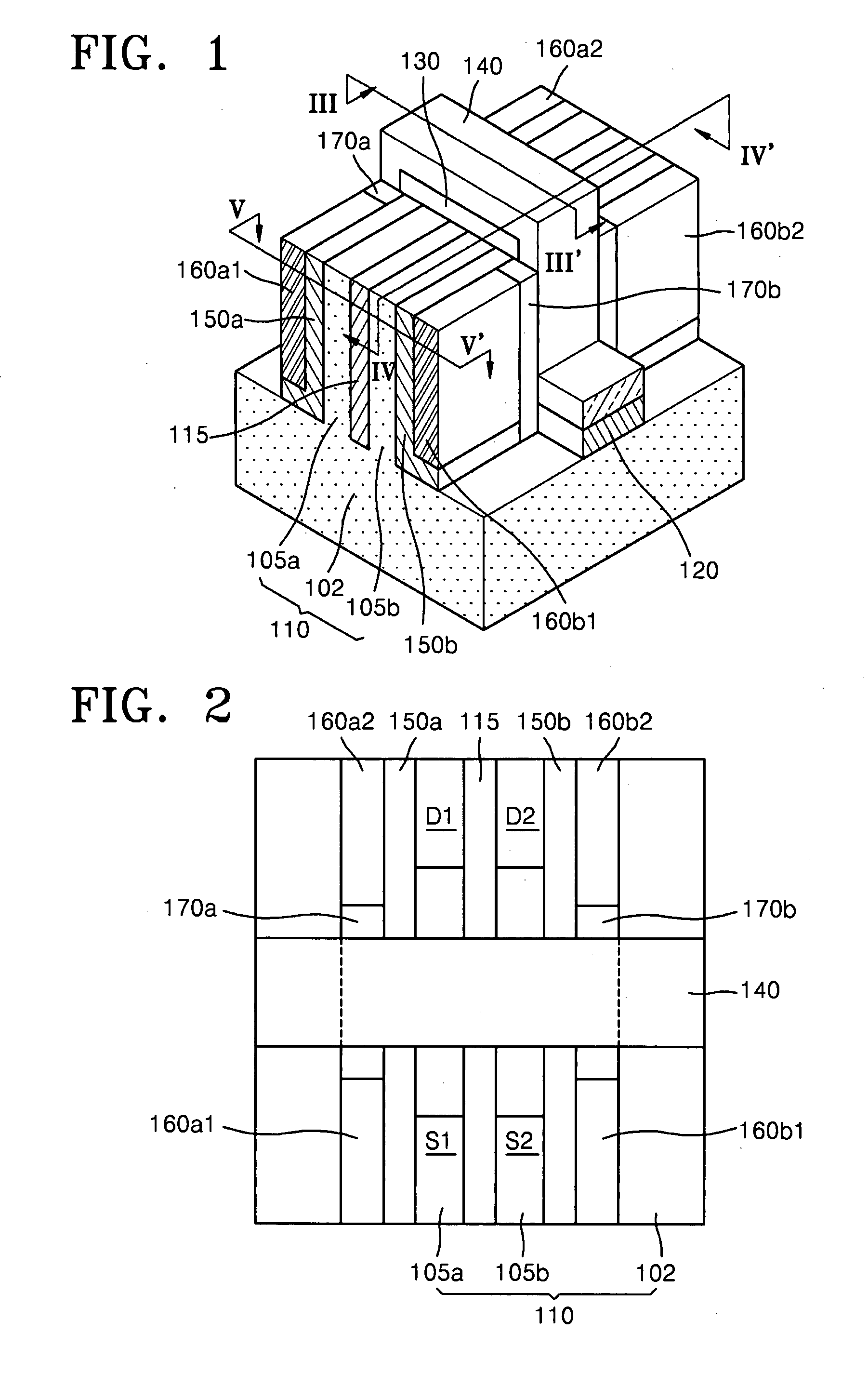
[0012]Programming the data may include using a hot electron injection (HEI) method. Data programming may be performed by supplying a turn-on voltage to a control gate electrode and by alternately applying currents in opposite directions to each other between a first source region and a first drain region and between a second source region and a drain region. Reading the data may include measuring the leakage current of a first source region and a first drain region and the leakage current of a second source region and a second drain region. In reading the data, a turn-off voltage may be supplied to a control gate electrode. Erasing the data may include using a hot hole injection (HHI) method. Data erasing may be performed by supplying a negative voltage to a control gate electrode and by supplying a positive voltage to at least one of a first source region, a first drain region, a second source region, and a second drain region. In erasing the data, the semiconductor substrate may be grounded.
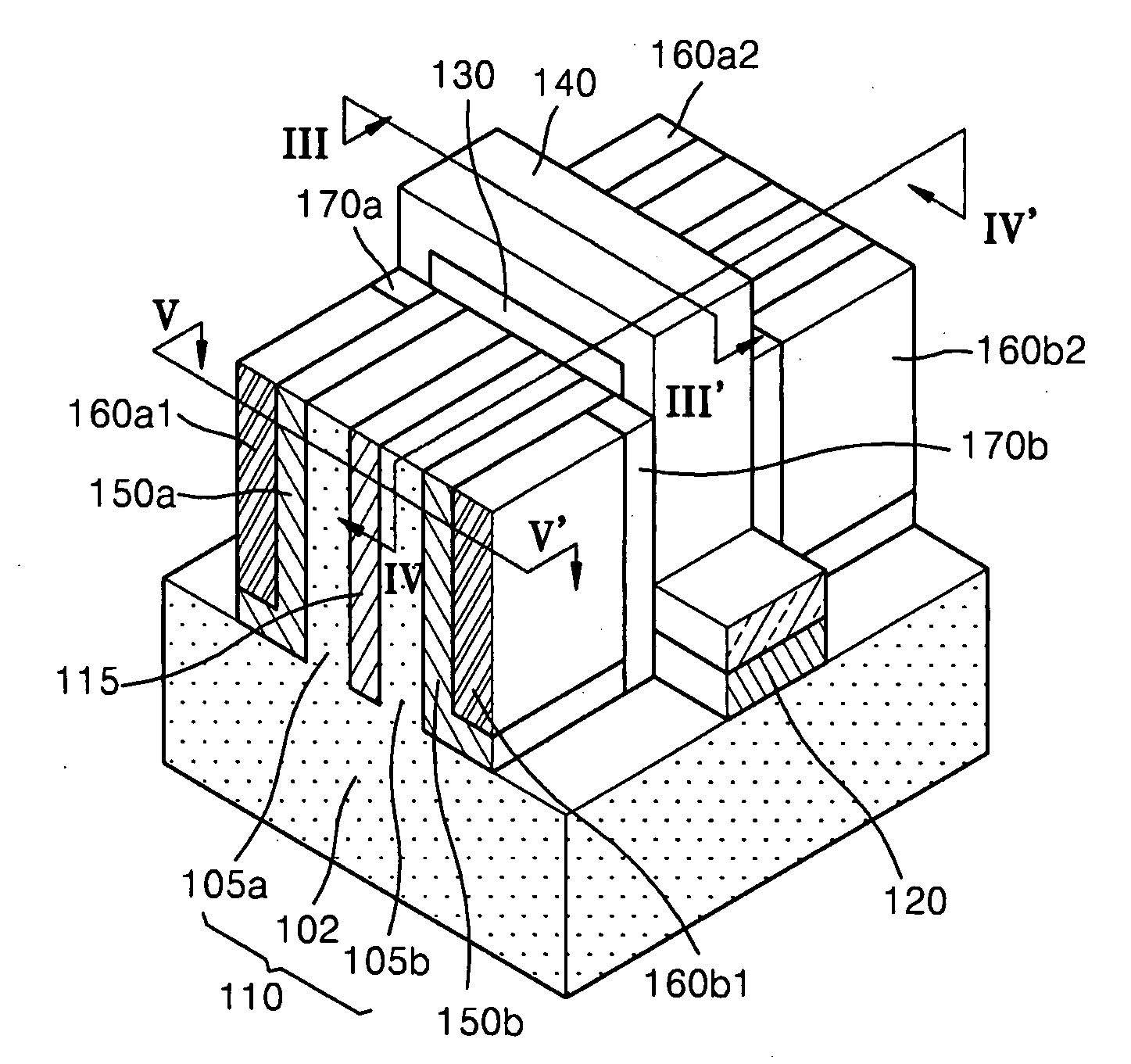
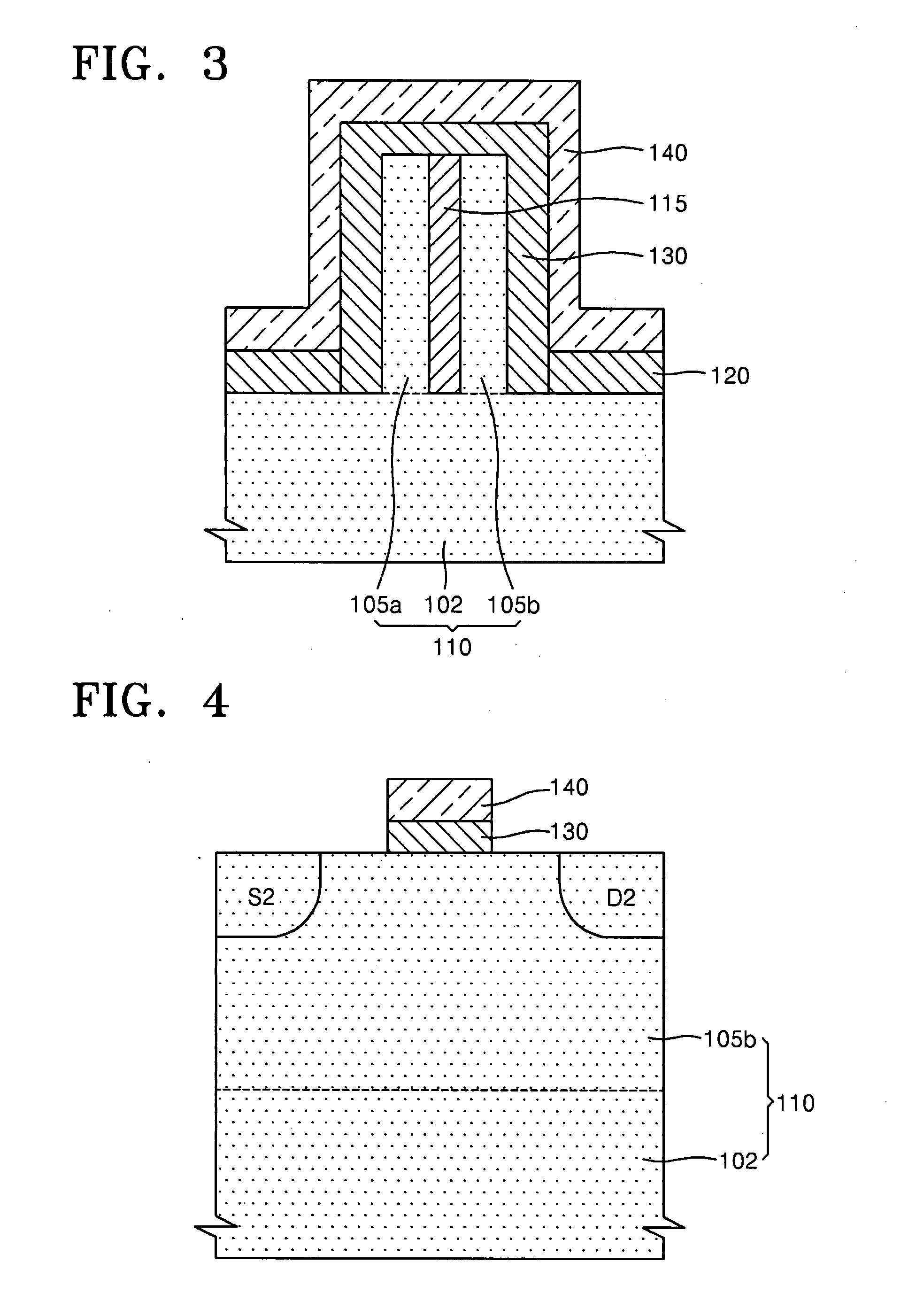
[0013]According to example embodiments, a method of manufacturing a nonvolatile memory device may include forming a first source region and a first drain region that are respectively in the first fin portions on both sides of a control gate electrode and respectively separated from the control gate electrode, forming a second source region and a second drain region on the second fin portions on both sides of the control gate electrode and respectively separated from the control gate electrode, forming first and second storage node layers with the control gate electrode therebetween and on the side of the first fin opposite to a buried insulating layer between first and second fins and forming third and fourth storage node layers with the control gate electrode therebetween and on the side of the second fin opposite to the buried insulating layer.
[0014]The method may further include providing a semiconductor substrate including the first and second fins, forming a control gate electrode on the sides of the first and second fins opposite to the buried insulating layer and extending onto the buried insulating layer, and forming a gate insulating layer between the first and second fins and the control gate electrode. The method may further include forming a first tunnel insulating layer between the first fin and the first and second storage node layers, and forming a second tunnel insulating layer between the second fin and the third and fourth storage node layers. The gate insulating layer and the first and second tunnel insulating layers may include an oxide layer. The thicknesses of the gate insulating layer and the first and second tunnel insulating layers may be different from each other.
[0015]The method may further include forming a first blocking layer between the control gate electrode and the first and second storage node layers, and forming a second blocking insulating layer between the control gate electrode and the third and fourth storage node layers. At least a portion of the first and second storage node layers may not overlap with the first source region and the first drain region. At least a portion of the third and fourth storage node layers may not overlap with the second source region and the second drain region. The semiconductor substrate may be an etched bulk semiconductor wafer. Forming the first, second, third, and fourth storage node layers may include at least one selected from the group consisting of a silicon nitride layer, dots of metal or silicon, and nano-crystals of metal or silicon. The semiconductor substrate may include a body and first and second fins that protrude from the body. The control gate electrode may be insulated from the semiconductor substrate.

Problems solved by technology

Conventional fin memory cells may have a stack structure in which a tunnel insulating layer, a storage node layer, a blocking insulating layer, and a control gate electrode are stacked at fins, but may be limited in reducing the spacing between the fins.

Method used


Image

  • Non-volatile memory device having four storage node films and methods of operating and manufacturing the same
  • Non-volatile memory device having four storage node films and methods of operating and manufacturing the same
  • Non-volatile memory device having four storage node films and methods of operating and manufacturing the same

Examples


Embodiment Construction

[0024]Example embodiments will now be described more fully with reference to the accompanying drawings, in which example embodiments are shown. Example embodiments may, however, be embodied in many different forms and should not be construed as being limited to the embodiments set forth herein; rather, these embodiments are provided so that this disclosure will be thorough and complete, and will fully convey the concept of example embodiments to those skilled in the art. In the drawings, the thicknesses of layers and regions are exaggerated for clarity.

[0025]It will be understood that when an element or layer is referred to as being “on,”“connected to” or “coupled to” another element or layer, it can be directly on, connected or coupled to the other element or layer or intervening elements or layers may be present. In contrast, when an element is referred to as being “directly on,”“directly connected to” or “directly coupled to” another element or layer, there are no intervening ele...


PUM


Abstract

A nonvolatile memory device that may operate in a multi-bit mode and a method of operating and manufacturing the nonvolatile memory device are provided. The nonvolatile memory device may include a first source region and a first drain region that are respectively in first fin portions on both sides of a control gate electrode and respectively separated from the control gate electrode, a second source region and a second drain region that are respectively formed in second fin portions on both sides of the control gate electrode and respectively separated from the control gate electrode, first and second storage node layers that are formed with the control gate electrode therebetween and on the side of the first fin opposite to a buried insulating layer between first and second fins, and third and fourth storage node layers that are formed with the control gate electrode therebetween and on the side of the second fin opposite to the buried insulating layer. The nonvolatile memory device may further include a semiconductor substrate including the first and second fins, a control gate electrode on the sides of the first and second fins opposite to the buried insulating layer and extending onto the buried insulating layer and a gate insulating layer between the first and second fins and the control gate electrode.

Description

PRIORITY STATEMENT[0001]This application claims priority under 35 U.S.C. §119 to Korean Patent Application No. 10-2006-0057088, filed on Jun. 23, 2006, in the Korean Intellectual Property Office (KIPO), the entire contents of which are incorporated herein by reference.BACKGROUND[0002]1. Field[0003]Example embodiments relate to a semiconductor device and methods of operating and manufacturing the same. Other example embodiments relate to a nonvolatile memory device including a fin type channel region and a method of operating and manufacturing the nonvolatile memory device.[0004]2. Description of the Related Art[0005]The volume of semiconductor components is becoming smaller and more quantity of data processing is being required. Accordingly, ways to increase the operation speed and the degree of integration of nonvolatile memory devices have been researched. For example, in a semiconductor device in which integration is improved using a fin-field effect transistor (fin-FET), the ope...

Claims


Application Information

Patent Timeline
Patent Type & Authority Applications(United States)
IPC IPC(8): H01L27/12G11C11/34H01L21/84H10B69/00
CPCH01L29/42332H01L29/7923H01L29/7887H01L29/7851H01L29/40114
Inventor PARK, YOON-DONGKIM, SUK-PILHYUN, JAE-WOONG
Owner SAMSUNG ELECTRONICS CO LTD
Learn More