Hybrid Field Effect Transistor and Bipolar Junction Transistor Structures and Methods for Fabricating Such Structures

a technology of bipolar junction transistor and hybrid field effect transistor, which is applied in the direction of transistors, semiconductor devices, electrical equipment, etc., can solve the problems of increasing fabrication complexity and cost, increasing the footprint of conventional bipolar junction transistors, and consuming a significant surface area of the active device layer

Inactive Publication Date: 2008-01-03
IBM CORP
View PDF5 Cites 38 Cited by
  • Summary
  • Abstract
  • Description
  • Claims
  • Application Information

AI Technical Summary

Benefits of technology

[0010]The present invention is directed to semiconductor device structures and fabrication methods that integrate non-planar bipolar junction transistors and field effect transistors on a common substrate. The device structures may comprise bipolar complementary metal-oxide-semiconductor (BiCMOS) device structures built

Problems solved by technology

For certain applications, the advantages of this integration justify the increased fabrication complexity and cost.
As a result, conventional bipolar junction transistors have a relatively large footprint that consumes a significant surface area of the active device layer.
The device footprint cannot be reduced

Method used


Image

  • Hybrid Field Effect Transistor and Bipolar Junction Transistor Structures and Methods for Fabricating Such Structures
  • Hybrid Field Effect Transistor and Bipolar Junction Transistor Structures and Methods for Fabricating Such Structures
  • Hybrid Field Effect Transistor and Bipolar Junction Transistor Structures and Methods for Fabricating Such Structures

Examples


Embodiment Construction

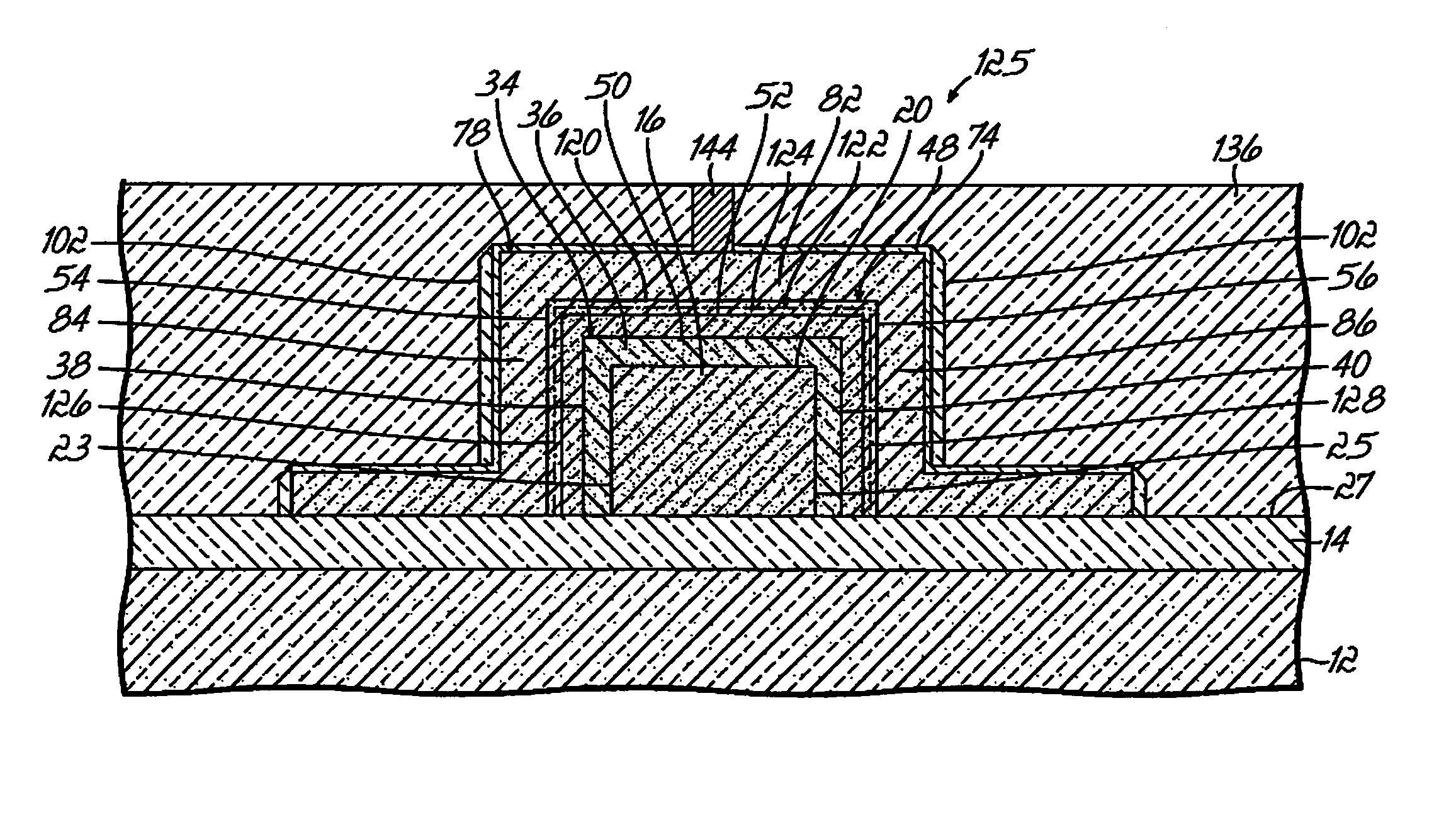
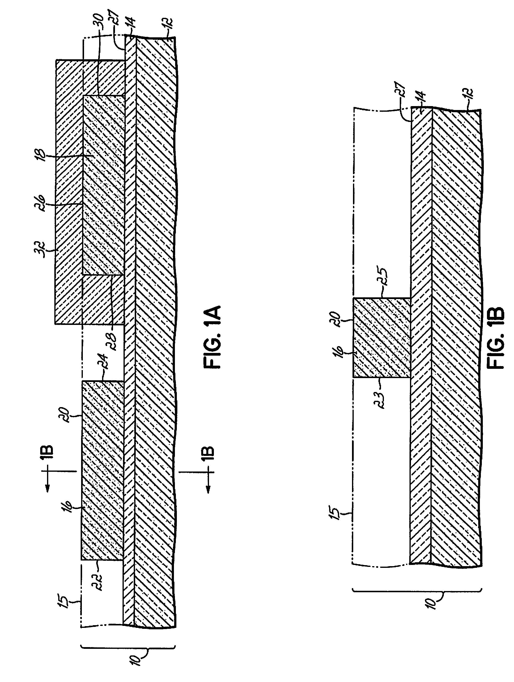
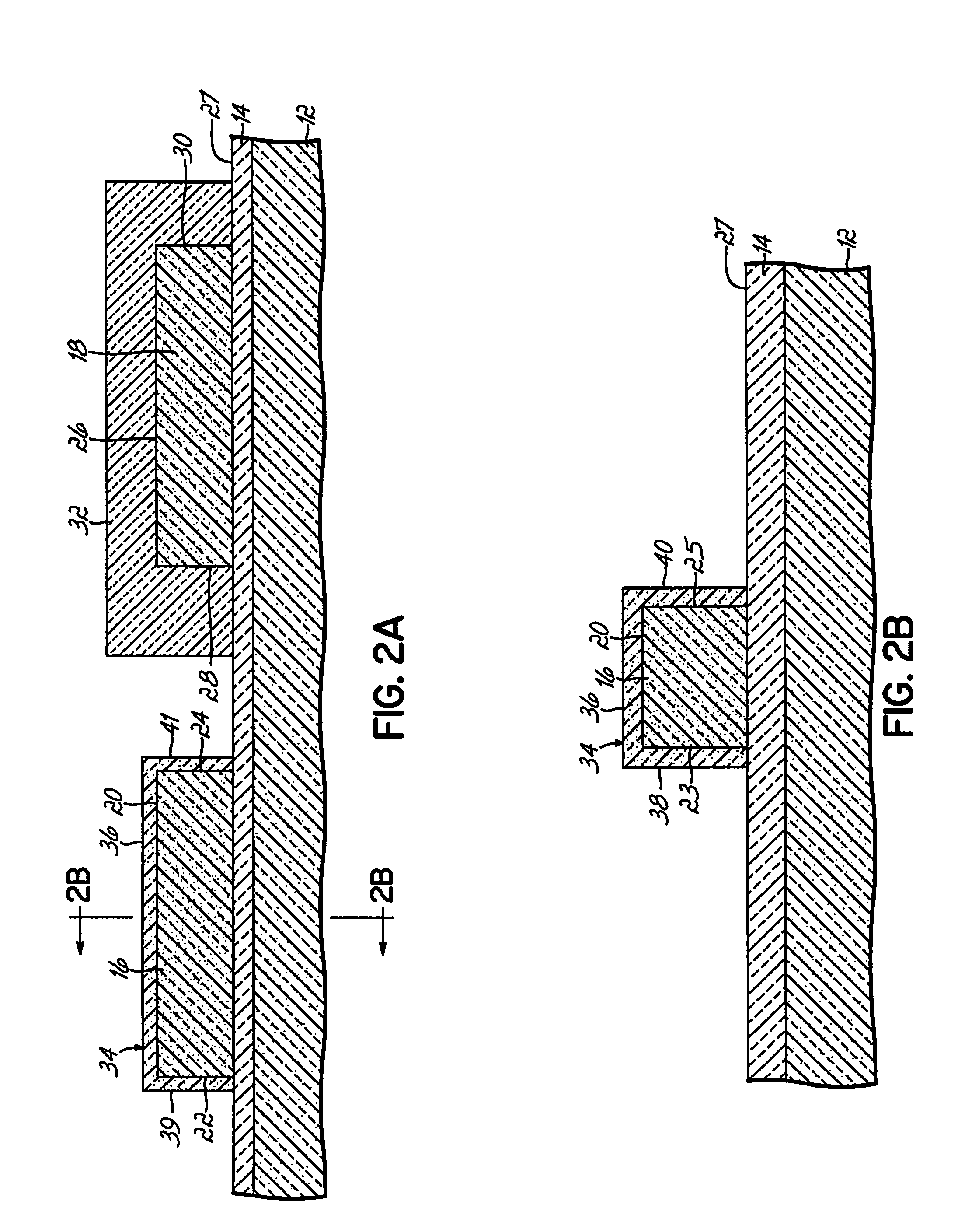
[0018]With reference to FIGS. 1A and 1B, an SOI wafer 10 comprises a handle substrate 12, a buried insulating layer 14, and a semiconductor or SOI layer 15 patterned by a conventional lithography and subtractive etching process to define a plurality of semiconductor mesas or fin structures, of which fin structures 16, 18 are representative and visible in FIGS. 1A, 1B. The fin structures 16, 18 are physically separated from the handle substrate 12 by the intervening buried insulating layer 14. The handle substrate 12 may be single crystal or monocrystalline silicon, although the invention is not so limited. The fin structures 16, 18, and the SOI layer 15 from which the fin structures 16, 18 originate, are considerably thinner than the handle substrate 12 and may be advantageously composed of single crystal or monocrystalline silicon, germanium, or silicon germanium. In one embodiment, the SOI layer 15 may be strained. The buried insulating layer 14 electrically isolates the semicondu...


PUM


Abstract

Semiconductor device structures that integrate field effect transistors and bipolar junction transistors on a single substrate, such as a semiconductor-on-insulator substrate, and methods for fabricating such hybrid semiconductor device structures. The field effect and bipolar junction transistors are fabricated using adjacent electrically-isolated semiconductor bodies. During fabrication of the device structures, certain fabrication stages strategically rely on block masks for process isolation. Other fabrication stages are shared during the fabrication process for seamless integration that reduces process complexity.

Description

FIELD OF THE INVENTION[0001]The invention relates generally to semiconductor device structures and fabrication methods and, in particular, to semiconductor device structures that integrate field effect transistors and bipolar junction transistors on a single substrate and methods of fabricating such hybrid semiconductor device structures.BACKGROUND OF THE INVENTION[0002]Planar bipolar complementary metal oxide semiconductor (BiCMOS) type integrated circuits combine the advantages of bipolar junction transistors (BJT's) and field effect transistors (FET's) on a single substrate. For certain applications, the advantages of this integration justify the increased fabrication complexity and cost. Bipolar junction transistors provide faster switching speeds, higher current drive, and have advantages for analog applications, such as better device matching, than field effect transistors. On the other hand, field effect transistors have been in the mainstream of device fabrication where high...

Claims


Application Information

Patent Timeline
IPC IPC(8): H01L29/76
CPCH01L21/8249H01L21/84H01L27/0623H01L29/785H01L29/66265H01L29/732H01L27/12
Inventor CHENG, KANGGUOHSU, LOUIS LU-CHENMANDELMAN, JACK ALLAN
Owner IBM CORP
Why Eureka
Try Eureka