

Liquid crystal display device and fabricating the same
- Summary
- Abstract
- Description
- Claims
- Application Information
AI Technical Summary
Benefits of technology
Problems solved by technology
Method used
Image

Examples
second embodiment
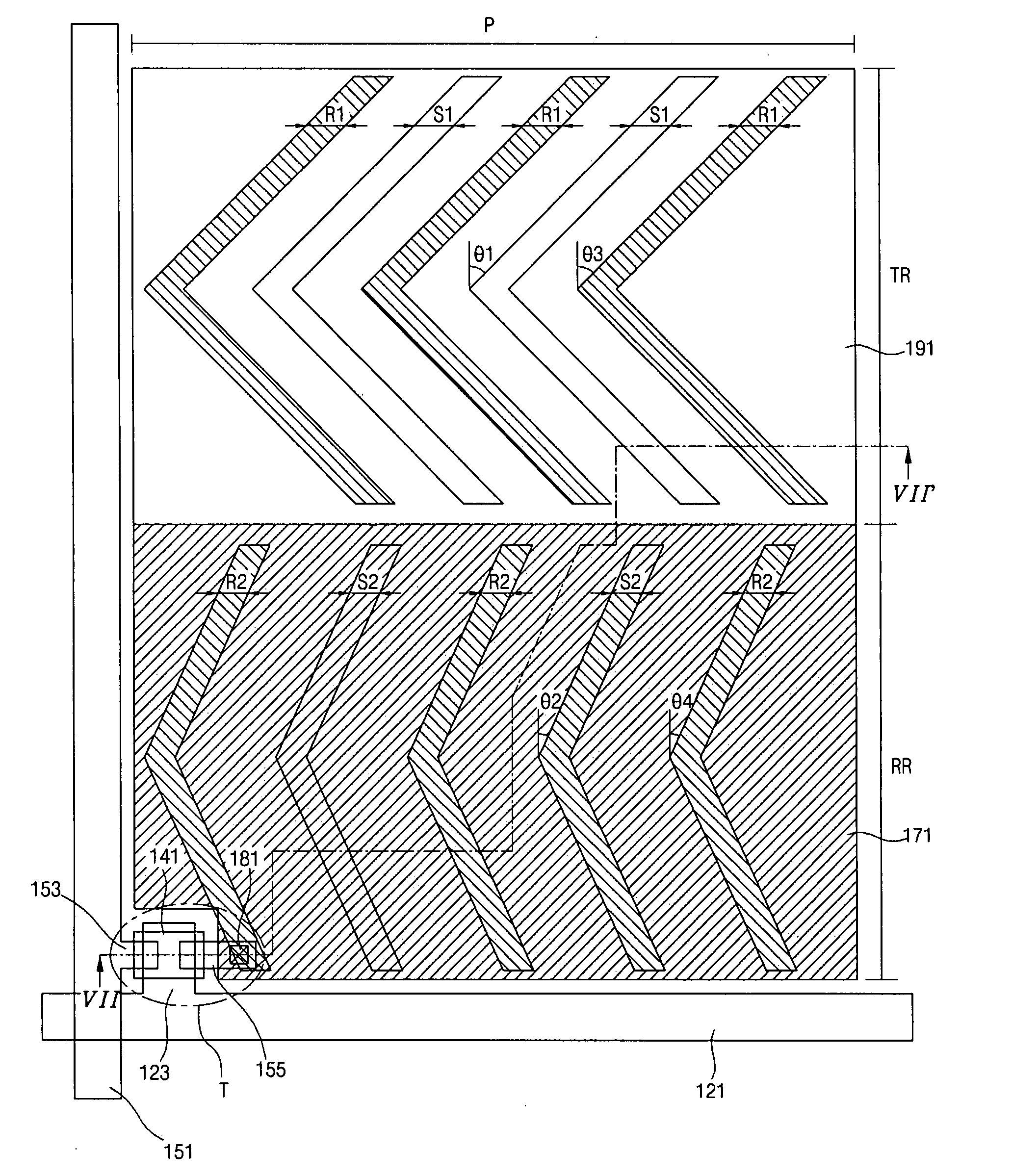
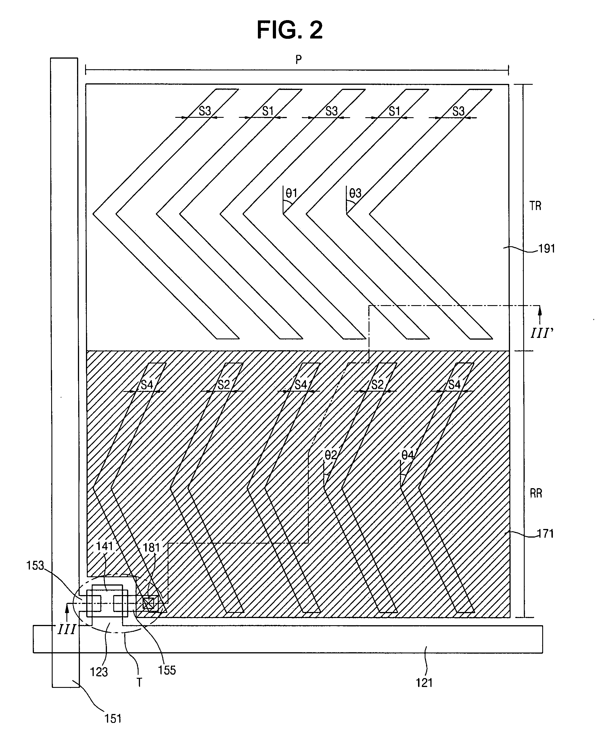
[0059]FIG. 6 is a plan view of a VA mode transflective LCD device according to a second exemplary embodiment of the present invention, and FIG. 7 is a cross-sectional view taken along line VII-VII′ of FIG. 6. The VA mode transflective LCD device shown in FIGS. 6 and 7 has substantially the same structure, except for forming a rib on the common electrode instead of using slits in the common electrode. The same parts as the first exemplary embodiment have the same references, and thus explanation for those parts in the second embodiment will be omitted.
[0060]As shown in FIGS. 6 and 7, the VA mode transflective LCD device has the single cell gap. In other words, the VA mode transflective LCD device has the same cell gap in the transmissive and reflective regions. The VA mode transflective LCD device includes the first and second substrates 110 and 210, and the liquid crystal layer 280 interposed therebetween. The liquid crystal layer 280 include the VA mode liquid crystal molecules. Th...
third embodiment
[0089]FIG. 11 is a plan view of a VA mode transflective LCD device according to a third exemplary embodiment of the present invention. The VA mode transflective LCD device according to the third exemplary embodiment has the same structure and the same manufacturing method as the first exemplary embodiment, except for a retardation film in the reflective region RR and in the transmissive region TR. The same parts as the first exemplary embodiment have the same references, and thus explanation for those parts in the third embodiment will be omitted.
[0090]As shown in FIG. 11, the VA mode transflective LCD device has a single cell gap, wherein a cell gap in the transmissive region TR is substantially the same as a cell gap in the reflective region RR. A first retardation film 310 is formed on an inner surface of the first substrate 110 adjacent to the liquid crystal layer 280, that is, on the transmissive electrode 191. A second retardation film 320 is formed on an outer surface of the ...
PUM
 Abstract
Description
Claims
Application Information