Miniature connector and preparation method thereof

A technology of micro connectors and manufacturing methods, which is applied in connection, contact box/base manufacturing, contact parts, etc., can solve the problems of high cost of SOI substrate, easy to be restricted to remove, and affect the plane shape of cantilever terminals. Achieve the best production yield, improve the production yield, and achieve the effect of good production yield

Active Publication Date: 2009-04-22
IND TECH RES INST
View PDF0 Cites 1 Cited by
  • Summary
  • Abstract
  • Description
  • Claims
  • Application Information

AI Technical Summary

Problems solved by technology

However, since the cost of the SOI substrate is relatively expensive, the production cost of the micro connector will increase significantly
On the other hand, in the process of using the SOI substrate to make micro-connectors, since the insulating layer between the two silicon material layers is thin (about 3 μm), part of the insulating layer between the two silicon material layers is removed to make the cantilever When terminals are used, the etchant used to remove the insulating layer is easily trapped in the thin gap between the disilicon material layers and is not easily removed. The surface tension of the etchant trapped between the disilicon material layers will generate Adsorption phenomenon (stiction) affects the out-of-plane shape of the cantilever terminal, resulting in poor yields of micro-connectors

Method used


Image

  • Miniature connector and preparation method thereof
  • Miniature connector and preparation method thereof
  • Miniature connector and preparation method thereof

Examples


Embodiment Construction

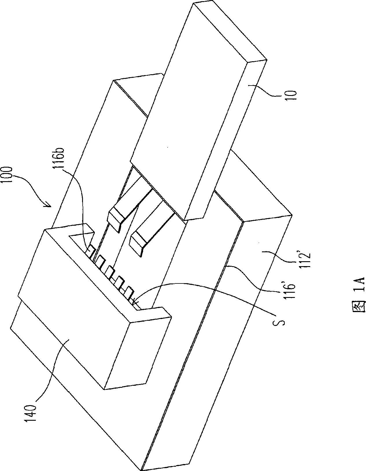
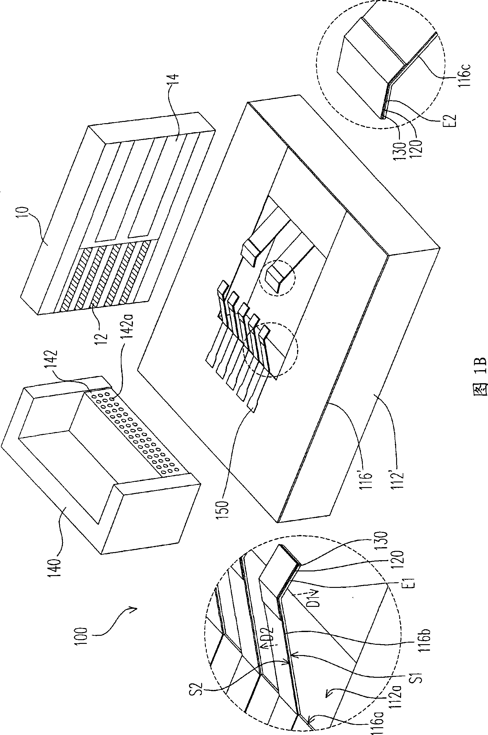
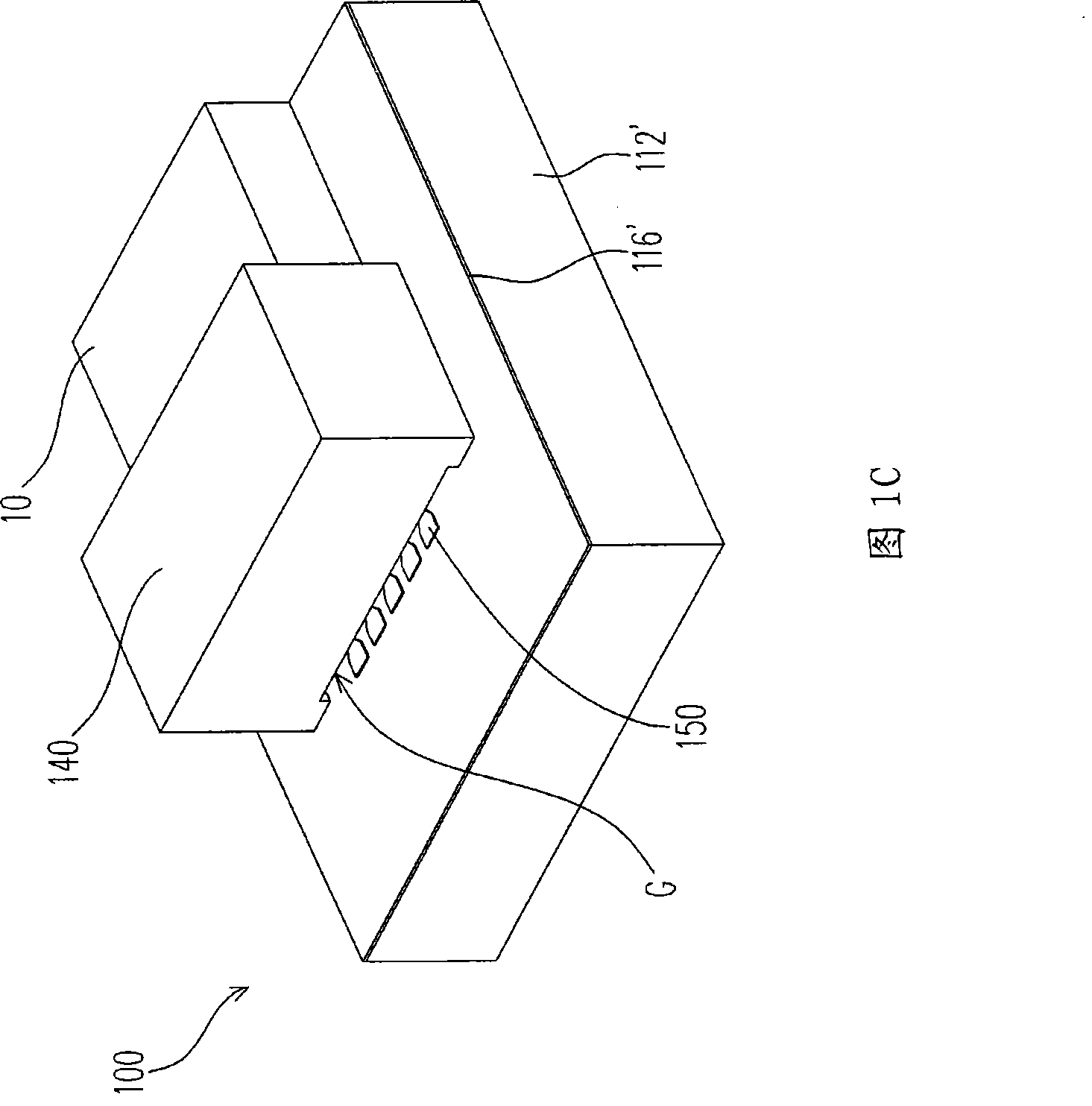
[0044] FIG. 1A is a schematic diagram of a micro connector and an insert according to an embodiment of the present invention, and FIG. 1B is an exploded view of the micro connector and the insert of FIG. 1A . Please refer to FIG. 1A and FIG. 1B at the same time. The micro-connector 100 of this embodiment is suitable for disposing in a light and thin electronic device, and the micro-connector 100 is suitable for inserting the insert 10, so that the electronic device has better performance. use efficiency. The micro-connector 100 of the present embodiment mainly includes a patterned silicon material layer 112', and the material is, for example, silicon dioxide (SiO 2 ), a patterned insulating layer (insulator) 116', at least one first stress layer 120, at least one second stress layer 130, and a cover 140. Wherein, the first stress layer 120 is, for example, a diamond like carbon (DLC) film or other suitable materials, the material of the second stress layer 130 is, for example, ...


PUM


Abstract

The invention discloses a miniature connector and a production method, the miniature connector comprises a patterned silicon material layer, a patterned insulation layer, at least a first stress layer, at least a second stress layer and a cover body, wherein the patterned insulation layer is matched and arranged on the patterned silicon material layer; the patterned silicon material layer is provided with a fist opening; the patterned insulation layer is provided with a second opening corresponding to the first opening and at least a cantilever terminal; and the cantilever terminal is protruded above the first opening. The first stress layer covers the end part of the cantilever terminal far away from the inner wall of the second opening, and so the end part is bent towards a direction. The second stress layer covers the cantilever terminal outside the end part, and so the cantilever terminal is bent towards the other direction. The cover body is matched and arranged on the patterned insulation layer, and covers the cantilever terminal.

Description

technical field [0001] The invention relates to a micro-electromechanical device and a manufacturing method thereof, and in particular to a micro-connector and a manufacturing method thereof. Background technique [0002] Generally speaking, the electronic device is usually equipped with a connector, and is electrically connected with the insertion part through the connector, so that the electronic device has better performance. However, with the advancement of science and technology, electronic devices tend to be thinner and lighter. The connector plastic body made by traditional molds and the conductive terminals made by stamping technology are not easy to be installed in thinner and lighter electronic devices. The known technology proposes a miniature connector suitable for being installed in light and thin electronic devices. Wherein, the miniature connector is provided with a plurality of conductive terminals, and the insertion part can be inserted into the micro conne...

Claims


Application Information

Patent Timeline
Patent Type & Authority Applications(China)
IPC IPC(8): H01R13/46H01R13/40H01R13/11H01R43/00H01R43/18
Inventor 章本华黄信瑀方维伦林欣卫
Owner IND TECH RES INST
Why Eureka
Try Eureka