Method of avoiding errors in flash memory

a flash memory and error prevention technology, applied in the field of flash memory storage systems, can solve the problems of low data retention time quality specification of mbc cells, lower reliability of mbc than sbc, and low performance of mb

Active Publication Date: 2008-02-07
WESTERN DIGITAL ISRAEL LTD
View PDF5 Cites 23 Cited by
  • Summary
  • Abstract
  • Description
  • Claims
  • Application Information

AI Technical Summary

Problems solved by technology

However, there are also some drawbacks to using MBC flash—the average read and write times of MBC memories are longer than of SLC memories, resulting in lower performance.
Also, the reliability of MBC is lower than SBC.
Thus, a disturbance in the threshold voltage (e.g. leaking of the stored charge causing a threshold voltage drift, interference from operations on neighboring cells, etc.) that may have gone unnoticed in SBC because of the large gap between the two states, might cause an MBC cell to move from one state to another, resulting in an erroneous bit.
The end result is a lower quality specification of MBC cells in terms of data retention time or the endurance of the device to many write / erase cycles.
There are several sources of errors in flash memory devices.
As mentioned above, one such source is the leakage of electrons out of the gate of a memory cell that might shift the cell's originally written state into another, incorrect state, resulting in one or more bit errors when reading the cell.
Unlike the leakage-type effect that results in slow accumulation of errors over long time periods in which data is stored in the flash device, the PD effect results in an immediate appearance of errors, immediately following the writing of data into the cells of the device.
A cell that is to be written has its bit line connected to low voltage, causing a large voltage difference across the cell, and resulting in the cell's threshold voltage getting increased, thus moving the cell to the right on the voltage axis of FIG. 1B and causing the cell's state to change.
However, even though cells that are not meant to be written have a lower voltage difference across them than cells that are meant to be written, the cells that are not to be written still have some voltage difference across them.
Therefore the need to apply higher control gate (i.e. word line) voltage to some cells results in higher voltage differences at the non-programmed cells.
Even though the cells are designed with the goal of not being affected by such anticipated voltage differences, in actual NAND flash devices such voltage differences stress the cells and might result in some of the cells changing their state even though this was neither intended nor desired.
To summarize the above explanation, PD is an effect in which when programming a page of cells, some cells that are intended to remain in the leftmost erased state end up in another state, resulting in bit errors when reading those cells.
Unfortunately, typical real-life user data is not random.
As a result, in real-life applications the problem of PD errors is more severe than what is expected based on random data patterns statistical calculations.
Relatively many cells will be in the erased state that is the most vulnerable state to PD errors, and therefore more PD errors than are predicted by random data distribution models will actually occur.

Method used


Image

  • Method of avoiding errors in flash memory
  • Method of avoiding errors in flash memory
  • Method of avoiding errors in flash memory

Examples


Embodiment Construction

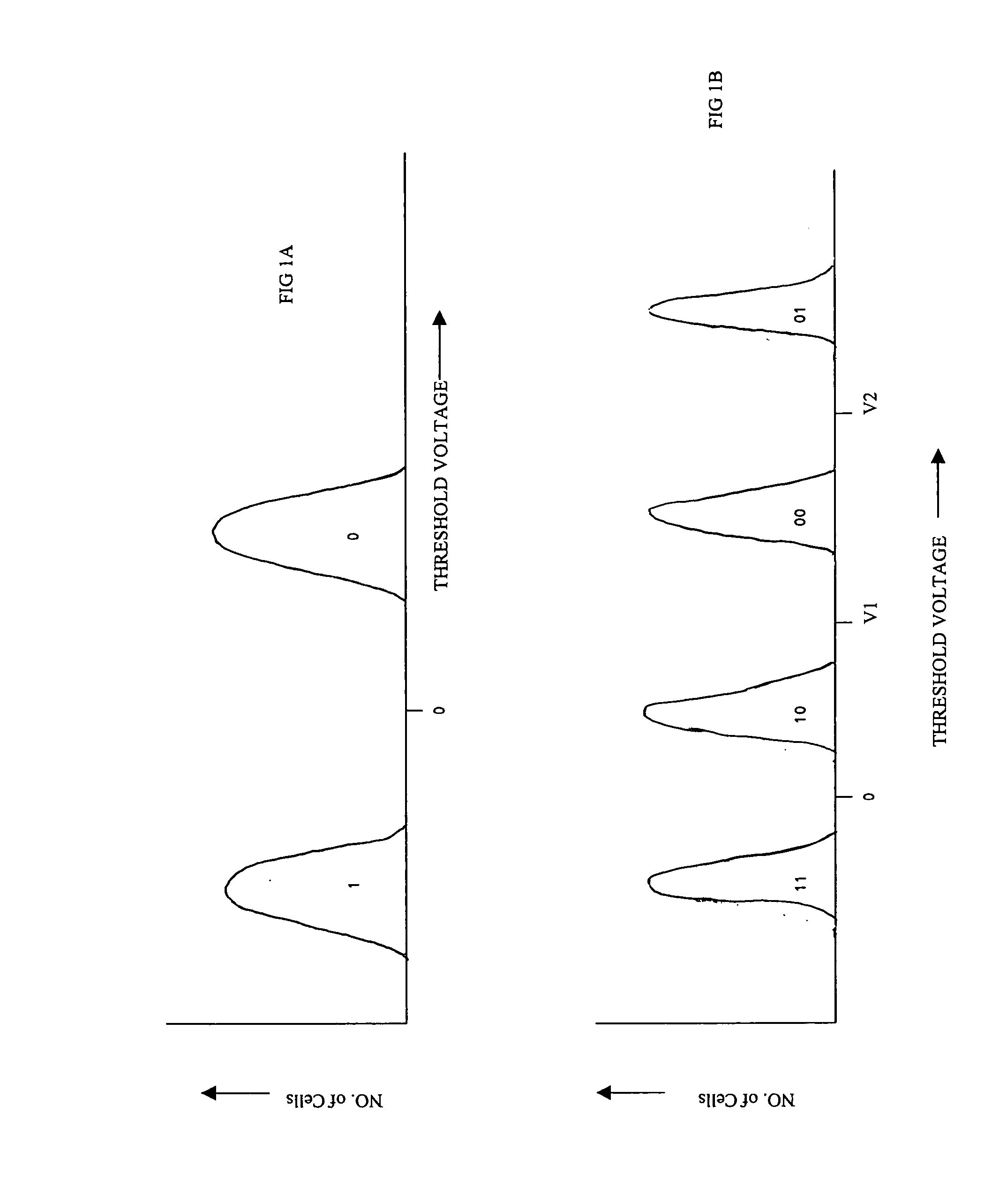
[0053]The present invention is a multi-bit-per-cell flash memory storage device that reduces the effects of PD errors, and the method by which the device reduces the effect of PD errors. The reduction of PD errors is achieved by making the cells' default all-one state a middle state along the threshold voltage axis, instead of the leftmost state as in prior art devices.

[0054]The principles and operation of a multi-bit-per-cell flash memory according to the present invention may be better understood with reference to the drawings and the accompanying description.

[0055]In the context of the example of FIG. 1B, a flash memory device of the present invention does not have the value of “11” represented by the leftmost state but for example by the third-from-the-left state. Thus the order of the states from left to right is not {“11”, “10”, “00”, “01”} as in FIG. 1B, but may be for example {“00”, “01”, “11”, “10”}. In this case, cells which are to contain values of “11”, which as we indic...


PUM


Abstract

Whenever N data bits are stored in a cell of a memory that programs each of its cells to represent any one of 2N different patterns of N>1 bits as a respective one of 2N ordered cell states, the N data bits are mapped to a transformed pattern of N bits according to a transformation that maps the pattern of the lowest state (typically all 1's) to a different pattern, and the cell is programmed to represent the transformed pattern. The transformation may invert all, some or only one of the bits of each pattern. Whenever the cells of the memory are read, the transformation is inverted.

Description

[0001]This patent application claims the benefit of U.S. Provisional Patent Application No. 60 / 820,960, filed Aug. 1, 2006FIELD AND BACKGROUND OF THE INVENTION[0002]The present invention relates generally to flash memory storage systems. More particularly, the present invention relates to flash memory storage systems in which the flash memory is capable of storing multiple bits per memory cell, and in which certain disturbance effects are minimized.[0003]Flash memory devices have been known for many years. Typically, each cell within a flash memory stores one bit of information. Traditionally, the way to store a bit has been by supporting two states of the cell—one state represents a logical “0” and the other state represents a logical “1”. In a flash memory cell the two states are implemented by having a floating gate above the cell's channel (the area connecting the source and drain elements of the cell's transistor), and having two valid states for the amount of charge stored wit...

Claims


Application Information

Patent Timeline
Patent Type & Authority Applications(United States)
IPC IPC(8): G11C11/34
CPCG11C7/1006G11C11/5628G11C2211/5647G11C16/3418G11C11/5642G11C16/10G11C16/26
Inventor SHARON, ERAN
Owner WESTERN DIGITAL ISRAEL LTD
Why Eureka
Try Eureka