Logic gate, scan driver and organic light emitting diode display using the same

a scan driver and logic gate technology, applied in the direction of static indicating devices, instruments, pulse techniques, etc., can solve the problem of difficult to form such a scan driver on the panel

Inactive Publication Date: 2008-02-14
SAMSUNG DISPLAY CO LTD
View PDF23 Cites 20 Cited by
  • Summary
  • Abstract
  • Description
  • Claims
  • Application Information

AI Technical Summary

Benefits of technology

[0024]At least one of the above and other features and advantages of the present invention may further be realized by providing a NAND gate, including a control transistor configured to control a connection between a second power source and an output terminal, a first electrode of the control transistor being coupled to the output terminal, a first plurality of transistors coupled in parallel between the first electrode of the control transistor and a first power source, the first plurality of transistors being configured to operate in correspondence with a plurality of signals, a second plurality of transistors coupled in parallel between the first electrode of the control transistor and a gate electrode of the control transistor, the second plurality of transistors being configured to operate in correspondence with the plurality of signals, and a third plurality of transistors coupled in series between the second power source and the gate electrode of the control transistor, the third plurality of transistors being configured to operate in correspondence with a plurality of bar signals.
[0025]The NAND gate may further include a capacitor coupled between the first electrode and the gate electrode of the control transistor.
[0026]At least one of the above and other features and advantages of the present invention may further be realized by providing a NOR gate, including a control transistor configured to control a connection between a second power source and an output terminal, a first electrode of the control transistor being coupled to the output terminal, a first plurality of transistors coupled in series between the first electrode of the control transistor and a first power source, the first plurality of transistors being configured to operate in correspondence with a plurality of input signals, a second plurality of transistors coupled in series between the first electrode of the control transistor and a gate electrode of the control transistor, the second plurality of transistors being configured to operate in correspondence with the plurality of input signals, and a third plurality of transistors coupled in parallel between the gate electrode of the control transistor and the second power source, the third plurality of transistors being configured to operate in correspondence with a plurality of input bar signals.
[0027]The NOR gate may further include a capacitor coupled between the first electrode and the gate electrode of the control transistor.

Problems solved by technology

However, because a conventional scan driver includes PMOS transistors and NMOS transistors, it is difficult to form such a scan driver on the panel.

Method used


Image

  • Logic gate, scan driver and organic light emitting diode display using the same
  • Logic gate, scan driver and organic light emitting diode display using the same
  • Logic gate, scan driver and organic light emitting diode display using the same

Examples


Embodiment Construction

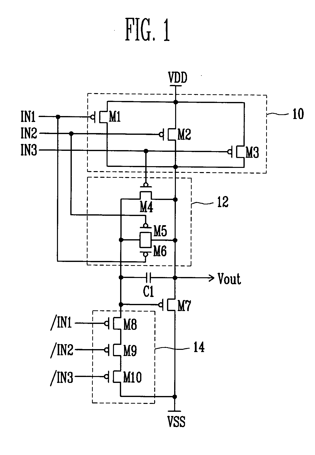
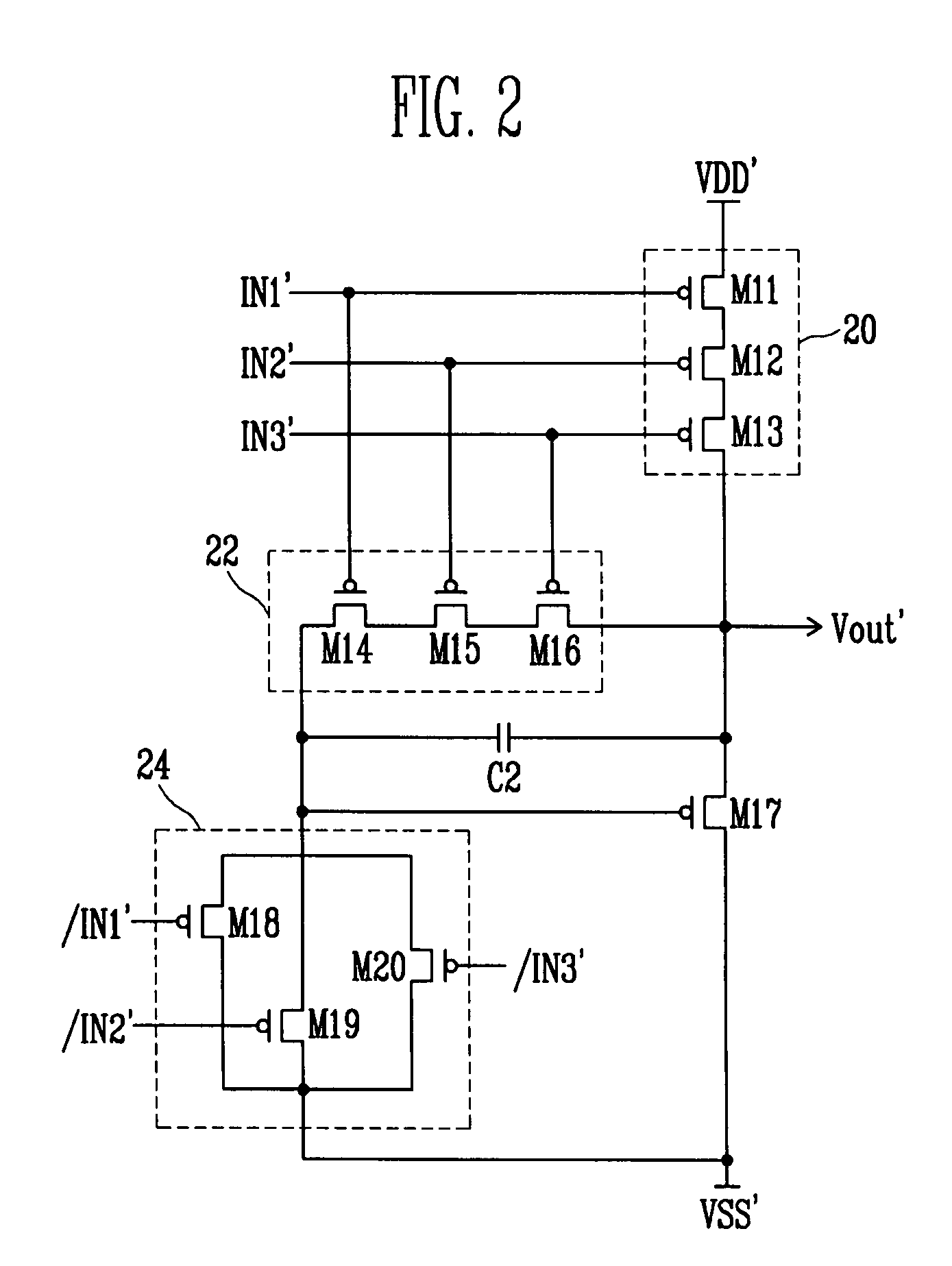
[0037]Korean Patent Application No. 10-2006-0074585, filed on Aug. 8, 2006, in the Korean Intellectual Property Office, and entitled: “Logic Gate, Scan Driver and Organic Light Emitting Diode Display Using the Same,” is incorporated by reference herein in its entirety.

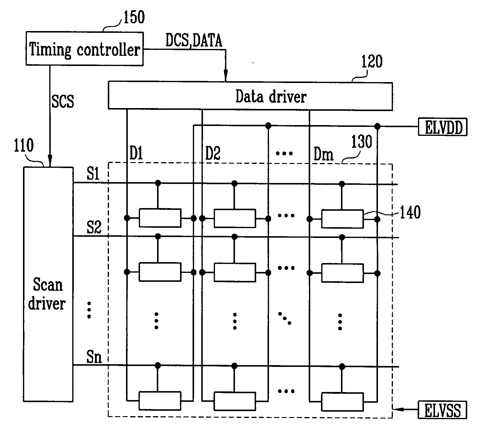
[0038]The present invention will now be described more fully hereinafter with reference to the accompanying drawings, in which exemplary embodiments of the invention are illustrated. The invention may, however, be embodied in different forms and should not be construed as limited to the embodiments set forth herein. Rather, these embodiments are provided so that this disclosure will be thorough and complete, and will fully convey the scope of the invention to those skilled in the art.

[0039]Where an element is described as being coupled to a second element, the element may be directly coupled to second element, or may be indirectly coupled to second element via one or more other elements. Further, where an element is de...


PUM


Abstract

An organic light emitting diode display, including pixel circuits coupled to respective data lines and scan lines, a data driver configured to supply data signals to the data lines, and a scan driver configured to provide scan signals to the scan lines, wherein the scan driver includes at least one decoder including a plurality of NOR gates, the decoder configured to provide a first plurality of signals, and a plurality of NAND gates coupled to respective scan lines, the NAND gates being configured to perform a NAND operation on the first plurality of signals and to provide scan signals to the scan lines, wherein all transistors in each of the NOR gates and each of the NAND gates are a same type of MOS transistor.

Description

CROSS-REFERENCE TO RELATED APPLICATION[0001]This application is related to co-pending U.S. patent application Ser. No. ______, entitled “LOGIC GATE, SCAN DRIVER AND ORGANIC LIGHT EMITTING DIODE DISPLAY USING THE SAME,” which was filed on Jul. 13, 2007.BACKGROUND OF THE INVENTION[0002]1. Field of the Invention[0003]Embodiments of the present invention relate to a logic gate, a scan driver and an organic light emitting diode display using the same. More particularly, embodiments of the present invention relate to a logic gate that may be realized using PMOS transistors, and a scan driver and an organic light emitting diode (OLED) display using the same.[0004]2. Description of the Related Art[0005]Recently, various flat panel displays exhibiting reduced weight and volume, which are disadvantages of cathode ray tubes (CRTs), have been developed. Flat panel displays include, e.g., liquid crystal displays (LCDs), field emission displays (FEDs), plasma display panels (PDPs), and OLED displ...

Claims


Application Information

Patent Timeline
Patent Type & Authority Applications(United States)
IPC IPC(8): G09G3/32H03K19/084H03K19/20
CPCG09G3/3266H03K19/09441G11C19/00G09G2300/0417G09G3/20G09G3/30
Inventor CHUNG, BO YONG
Owner SAMSUNG DISPLAY CO LTD
Why Eureka
Try Eureka